System Assembly and Testing
Here are most of the items that are required to assemble a complete Mk2 PV Router using my PCB-based hardware.
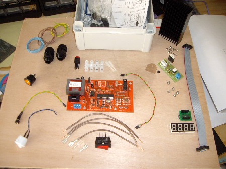
Central section, top to bottom:
- Schneider enclosure (external dimensions in mm: height = 165, width = 195)
- neon indicator (no longer used, it has been replaced by a LED assembly)
- mains connector (57A, 4-way) + M3 mounting screws
- control cable (red/green to link between the 'main' and 'output' PCBs)
- main board, assembled
- 1.5mm brown multi strand cable for internal high-power wiring
- 16A over-ride switch (SPST, illuminated)
- female spade connectors with covers (x3)
Right hand side, clockwise, from top:
- ABL heatsink & M3 mounting screws (heatsink depth = 20 mm)
- completed output board with triac mounting kit
- M3.5 screws for PCBs (4 for main board, 1 for the output board)
- display module (4-digit display, adapter plate, and ribbon cable)
Left hand side, clockwise, from bottom:
- mode switch (SPST), pre-wired to 2-way SIL connector
- mono 3.5mm jack socket, pre-wired to 2-way SIL connector
- mains switch (1A, DPST, illuminated)
- 16mm glands (x2)
- multi-strand cable for internal low-power wiring
Here is a parts list for the complete router as a spreadsheet.
When assembling a complete Router system, the first stage is to work out exactly where everything is to go and then make the necessary holes in the enclosure. It may be helpful to read through the whole of this section first before starting the assembly process.
Here are the recommended hole sizes for components that I supply:
- circular hole for triac: 32 mm diameter
- DPST mains switch (illuminated): 20 mm diameter
- SPST switch (white), if needed: 20 mm diameter
- gland for power cable: 16 or 20 mm diameter
- mono jack socket: 8 mm diameter
- LED bezel: 6.5 mm diameter
- 4-digit display: 50 x 19 mm approx
- 16A "constant" SPST switch: 30 x 10 mm approx
In the following sequence, I've used an ABS "Thalassa" enclosure from Schneider Electric, type NSYTBS19168. A polycarbonate version is also available, type NSYTBP19168. Two of the PCBs can be screwed directly to the internal mounting points of these enclosures.
NB. Throughout this Build Guide, I've assumed that the enclosure will be mounted horizontally. But if space does not permit this, it can be mounted vertically as shown below.
∗∗∗ A complete Mk2 unit in 'portrait' orientation is now featured on the Photo Gallery page ∗∗∗
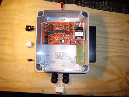
With the transformer being hidden behind the heatsink, this arrangement has plenty of wall-space in which to mount the various external components.
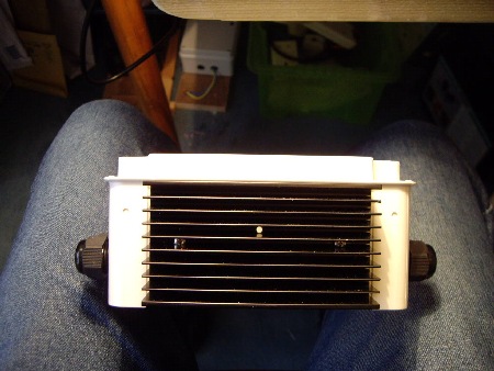
Here, the mounting hole for the triac is located centrally across the width of the box and heatsink, and is one 'valley' (6mm) above the mid-point of the heatsink.
NB. In the photo above, the heatsink is located as high as possible, with its upper edge tight against the protruding lip. This means that the triac has to be mounted at the extreme end of its leads. Having assembled several boxes, I've found it better to lower the heatsink slightly - just a few millimeters - which suits the location of the triac better.
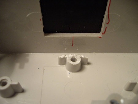
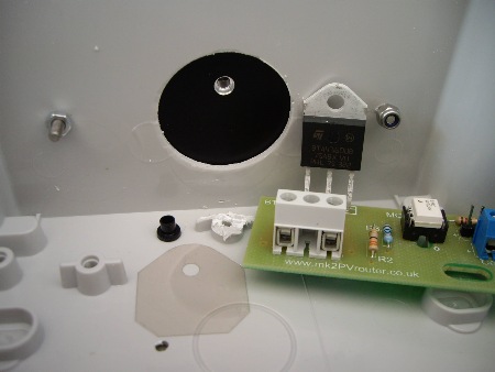
When using a Schneider enclosure and ABL heatsink, the centre of this hole needs to be approximately 30mm from the base of the box.
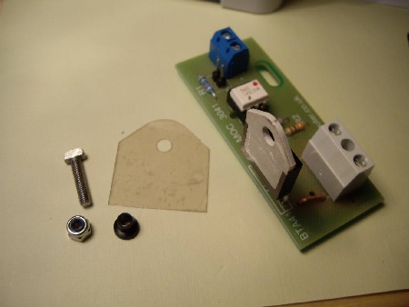
An insulating washer takes minimal space so should not noticeably affect the triac's location.
A smear of thermal paste may be helpful too.
As shown here, the head of each screw will need to be filed to fit between the fins of the heatsink.
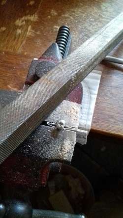
With a large file, this process does not take long.
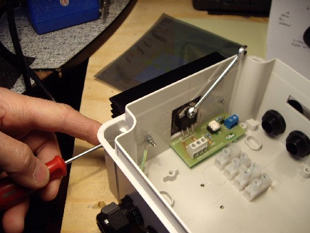
Make sure that the plastic bush is properly seated before the nut is fully tightened.
The central 3mm hole in the heatsink will need to be widened to 4mm to accommodate the plastic bush. This operation will already have been done for any pre-drilled heatsinks that I supply.
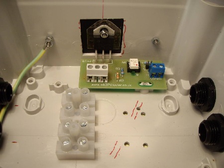
The two screws for the connector block need to sit either side of this ridge.
By drilling these holes from the rear, it should be possible to get them in the right place at the first attempt!
In the above photo, the location of the connector block is for when external power wiring is to appear from the right hand side of the box (in this case, the pair of glands on the left-hand-side would not be used).
In the photo below, the location of the connector block is for when external power wiring is to appear from the left hand side of the box (in this case, the pair of glands on the right-hand-side would not be used).
Depending on whether the heatsink is to be situated on the left-hand or the right-hand side of the enclosure when mounted on the wall, the connector and gland locations can be chosen to allow cable access from either above or below.
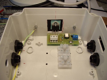
Whichever type of mounting kit is used, the heatsink will need to be earthed.
In the above photos, the earth connection is made via an M3 screw to the front face of the heatsink. A more direct approach is to fit the eathing tag directly to the rear face of the heatsink, as shown below:
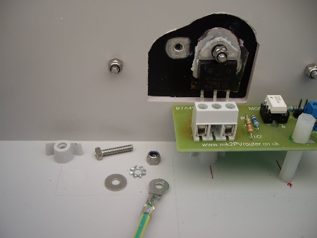
A serrated washer should ensure good contact.
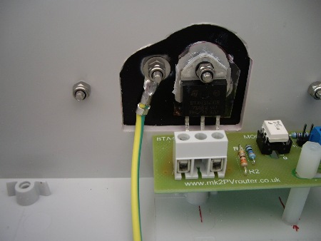
A self-tapping screw may be an easier approach than the M3 bolt that I have used here.
In harsh environments, the corrosive effect of dissimilar metals may need to be to taken into consideration.
Various external components will need to be mounted in the walls of the enclosure, their physical positions being dependent on the local circumstances. Some of these components are for mains; others are for low voltage signals. To prevent dust ingress, I would recommend having the override switch at the bottom.
When all of the mounting holes have been made, the assembled control board can be screwed into place using the four screws that are supplied with each enclosure. The internal wiring between the various components is shown in this diagram:
The next section is intended to give an overview of how everything is connected together. A detailed order in which to proceed with the mains wiring is suggested further down this page (immediately after the photo of the labels that I use).
The neon that was originally specified is no longer available. It has been replaced by an LED assembly.
Three of the low voltage components are connected to the main board via low-voltage cable and 2-way SIL sockets:
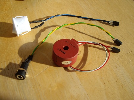
The jack-socket goes to the "CT1" connector.
The red 'bobbin-style' CT goes to the "CT2" connector.
For the components that carry mains voltage, I suggest that they are connected as shown on the diagram, internalWiring_1.pdf which is available on the Downloads page. When configured in this way, the completed Router should be able to pass the standard electrical tests for Continuity and Insulation Resistance.
NB.
The following sequence includes the fitting of a 230V neon into the Switched Live wiring. That component is no longer available so I now supply an LED and series resistor which provides an alternative way of showing when the load is active (i.e. on). The LED assembly is normally connected to the low-voltage side of the output stage PCB. It must not be connected to 230 Volts!
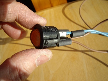
This is the amber coloured round DPST mains switch with illumination. If using a switch of this type, the supply wires must go to the outer pair of contacts.
The pair in the centre are for the switched outputs.
The amber DPST switch is no longer available but I have since found a green equivalent which is now supplied with all kits. At one stage, neither round type was available so the rectangular type in the next two images was supplied instead.
This replacement switch also has four terminals. The pair of terminals that are closest together are for the permanently live feed (Line and Neutral). The pair that are furthest apart are the switched live terminals (i.e. Switched Line and Switched Neutral).
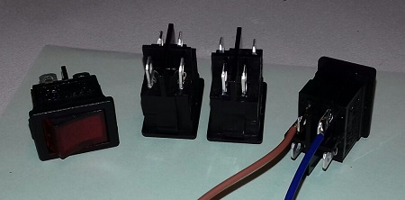
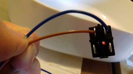
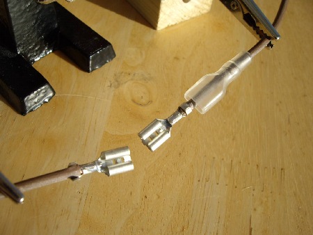
With the non-crimp variety, the wire can be soldered into place, then secured with pliers.
If using a plastic cover, it needs to be threaded onto the cable first.
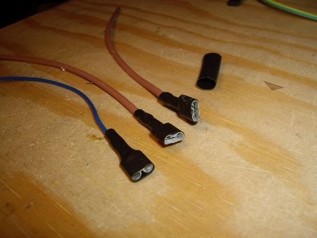
To avoid the internal wiring being disturbed during installation, all of the internal connections should be made on the side of the connector block that is furthest away from the glands.
At the 4-way connector block, the Line and Switched-Line terminals each supply three wires. When assembling the prototype unit, I found this operation to be quite challenging. But here is an easy way:
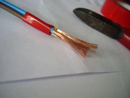
then tape them together without pre-twisting any of the copper cores.
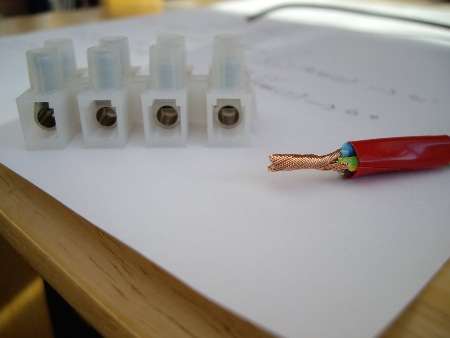
After trimming to the required length, this bundle should be an easy fit within the connector block.
NB. The different coloured wires that I used here were just to demonstrate the principle. Normally, they would all be the same colour.
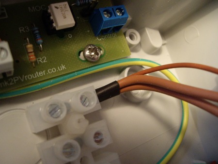
For the high-power wiring, it is important that the wires are firmly retained within their connectors.
Slackening and re-tightening the screw while gently moving the wire(s) can help to prevent any subsequent movement.
NB. Please note that stranded wire on power cables should NOT be tinned before being inserted into any type of pressure-activated connector (i.e. screw or crimp). Pre-tinning the wire ends could cause the connection to work loose over time and arcing to occur.
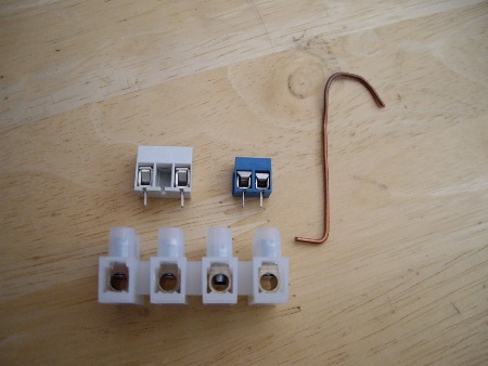
Make sure that the grub screws are fully retracted first.
To show the state of each load, an LED with a series resistor is normally fitted to the low-voltage side of the output stage. This is how I assemble an LED cable:
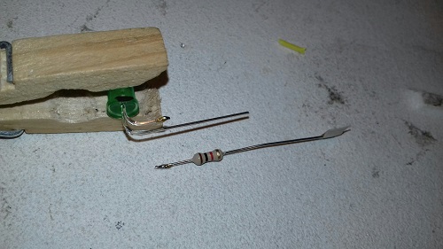
- mark the negative side of the LED (where the "flat" is) and bend both legs around at 90 degrees;
- Trim the negative leg of the LED and one end of the 1K0 series resistor to the required length;
- "Tin" both trimmed ends with solder.
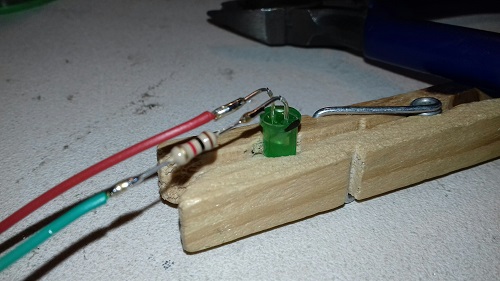
- then:
- solder the two tinned ends together;
- trim the protruding leg of the LED and the resistor to the required length;
- solder wires of the appropriate colours to the trimmed ends;
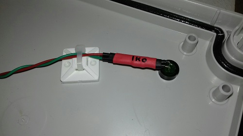
and finally:
- add heatshrink tubing to suit and, note the value of the series resistor;
- gently twist the wires and attach a 2-way SIL connector at the other end of the cable;
- add some hot-glue around the exposed legs of the SIL connector.
With everything in its place …
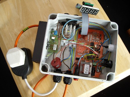
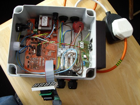
To assist with the testing process which follows, I've connected some 3-core flex in place of the incoming and outgoing supplies. These temporary cables are terminated with a 13A plug and trailing socket respectively. Once installed, these cables would normally be 2.5 T&E.
Now for a closer look at the high-current mains wiring:
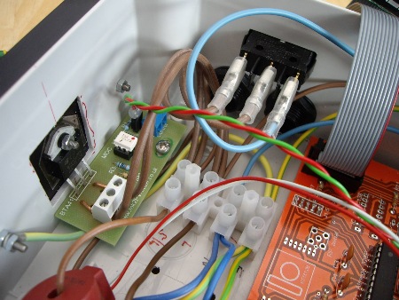
When either of these circuits is 'on', the permanently live Line terminal is connected to the switched-Line outlet for the load.
(The red/green control cable which runs between the two PCBs can also be seen here.)
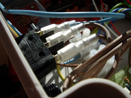
These connectors have not yet been pushed fully home.
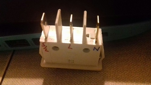
- the central terminal, marked "1", is for the permanently 'live' Line connection;
- the outer terminal marked "2" is for the 'switched live' Line connection;
- the outer terminal marked "3" is the Neutral connection for illumination only;
Now for the low-current mains wiring:
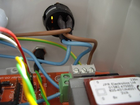
If the heatsink and switch were on the opposite sides, no crossover would be necessary.
This type of DPST switch has four terminals and a wire is connected to each of them. The bright stripe in this photo is a gap through with the internal workings of the switch can be seen.
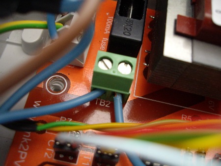
A switched-Neutral feed for these two components can be conveniently provided by TB2.
NB. The high-voltage neon is no longer fitted. It has been replaced by an LED and series resistor which is connected to the low-voltage control circuit.
And now for the low-voltage wiring. When fully populated, each of the four 2-way SIL connectors will be in use, as shown below:
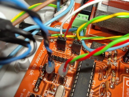
The red & white pair at "CT2" is for the internal CT.
The red & green pair at "trigger" is the control pair for the output board.
The blue & black pair at "mode" is for the switch which selects the output mode.
(Not used for all Mk2 applications)
These SIL connectors are greatly improved with a dab of hot glue to seal the wires in place. As can be seen from the above photo, two of mine have yet to receive this treatment.
The red/green cable for the control signal runs between the "trigger" connector on the main board and the "control" connector on the output board. At the 'main' board end, there needs to be a 2-way SIL connector, as shown above. At the 'output' board end, there can be a similar 2-way SIL connector, or these wires can be screwed into the 2-way terminal block marked "control".
NB. If a lid-mounted LED is to be used instead of a neon to show when the load is on, the 2-way SIL strip on the output board can provide a convenient connection point. In that case, it may be helpful to wire the control cable to the 2-way terminal block.
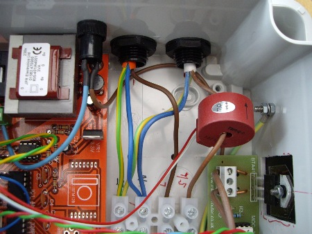
Here, it is around the switched-Line cable.
The arrow on the CT has no relevance for this application. If the signal is not the right way up, just reverse the SIL connector at CT2.
The above location for the internal CT is fine for when the system is being assembled and installed within the same operation. Before the outlet cable is screwed into place, either of its 'live' cores is passed through the internal CT.
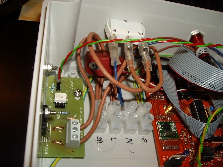
When the assembly and installation stages are being done separately, it may be better for the internal CT to form part of the internal wiring, as shown in the photo below. The area for the external cabling is then completely clear.
And finally, some views from the outside:
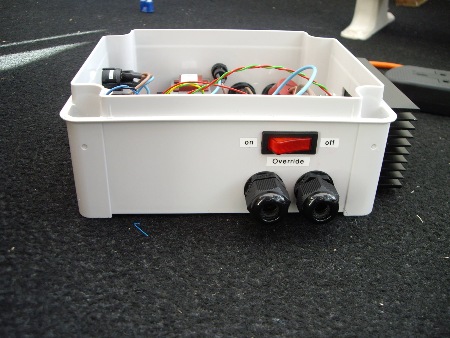
If the T&E cables need to enter from below, the wiring requires a bit more care, but it can be done.
Because this unit has its heatsink on the right, most of the controls are on the left-hand side:
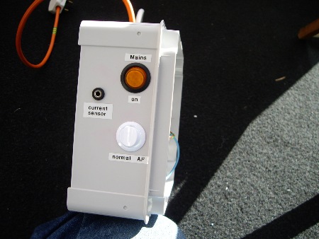
The other switch, for selecting between "normal" and "anti-flicker" modes, is operated in a side-to-side manner.
The 3.5mm socket is for the external CT.
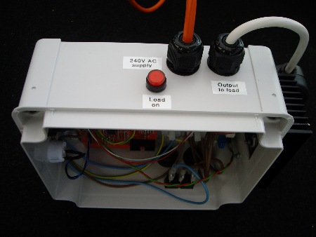
But it's fine for the cable entry points and the neon.
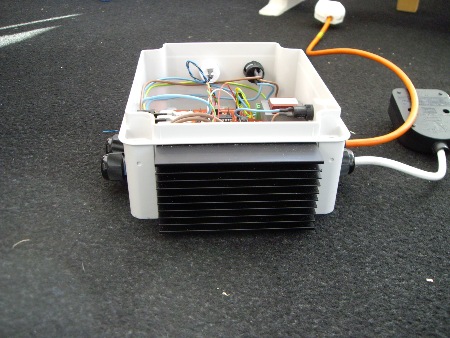
For a 110 mm length, as shown here, this heatsink profile from ABL has a thermal resistance of just under 1.5 degC/Watt with passive cooling.
I can supply heatsinks of this type which are pre-drilled.
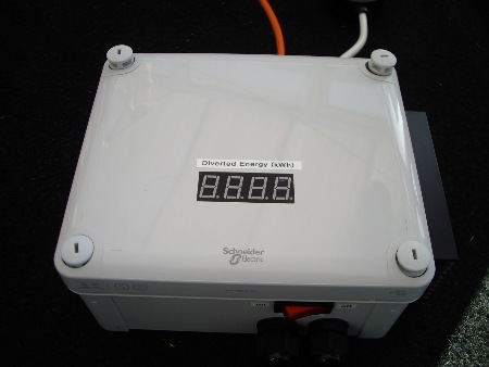
It is also a good location for an LED to show when the load is active. An LED (with its series resistor) has not been fitted here because this box includes a neon indicator.
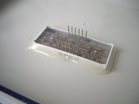
To improve the joint, I roughen both of the surfaces first.
Make sure the display is the right way up before glueing it into place!
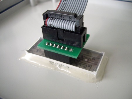
NB. As mentioned on the Display PCB page, I now recommend soldering the adapter plate directly to the pins of the display module. This provides a more reliable means of connecting to them.
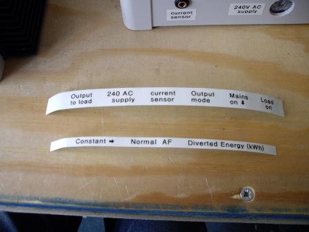
For UK use, the "supply" label should read "230V AC"
∗ ∗ ∗
The order in which I usually assemble the internal wiring for a Mk2 system is as follows. Two set of photos are provided for units in which the heatsinks are on opposite sides. Depending on the layout of the various components, many different configurations of wiring are possible, but they can all be approached in a similar way. In the accompanying photos, the two sequences are denoted Right and Left. So "W3-R' is wiring stage No 3 for the unit with the heatsink on its right hand side.
| 1. Add the two earthing cables | W1_L | W1_R |
| 2. Add the mains switch, leaving the "Line" cable unattached | W2_L | W2_R |
| 3. Complete the "Line" wiring | W3_L | W3_R |
| 4. Add the neon, leaving the switched-line cable unattached | W4_L | W4_R |
| 5. Complete the switched-line wiring, which may pass through CT2 | W5_L | W5_R |
| 6. Add the low voltage cables and the neutral for the override switch | W6_L | W6_R |
| 7. Retain any loose cable to the sides of the enclosure | W7_L | W7_R |
(stage 4 is no longer needed as the neon has been replaced by an LED assembly)
∗ ∗ ∗
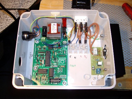
With the layout of this box, the fixed internal wiring is probably as compact as is possible.
Although a second CT has not been fitted, sufficient slack has been left in the switched-line wiring so that this could be done later.
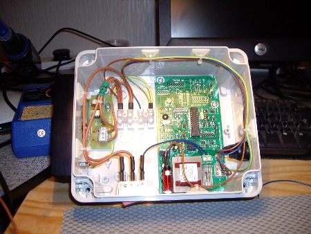
As with the above unit, sufficient slack has been left in the switched-line wiring so that CT2 can be added later.
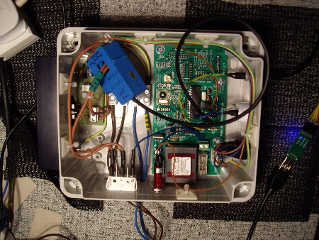
A clip-on CT has been fitted for test purposes. This allows the diverted power to be measured for datalogging via radio (this unit does not have a display).
Safety Warning:
To continue with this build sequence, access to 230V mains voltage is required. Please take great care, and do not undertake this activity unless you feel confident to do so.
Now that the Router is fully assembled, some additional tests can be performed.
Testing the 4-digit display.
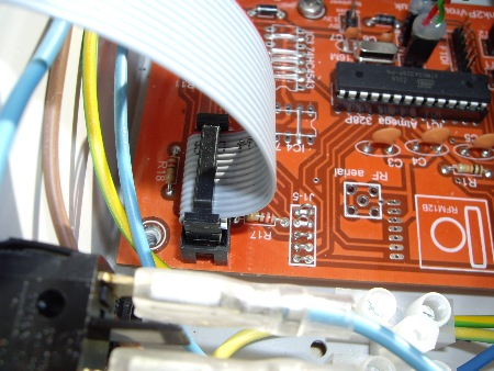
… just run the sketch
[NB. When a file is downloaded from this website, it is automatically "opened" within a suitable editor or browser. To use a software sketch, the entire content of the displayed file should be copied and saved as a local file using the name that appears here. Because it has the suffix ".ino", that file will then be recognised as an Arduino source file by the Arduino IDE].
The demo_bothDisplays sketch needs to be configured for whichever version of the hardware it is running on. This involves a one-line change near the start of the code. If ICs 3 & 4 are in use, the line #define PIN_SAVING_HARDWARE needs to be included; otherwise, this line needs to be commented out (by adding "//" at the start of the line). Most sketches that use the 4-digit display need to be set up in a similar way.
The behaviour of this sketch is determined by the state of the boolean flag, EDD_isActive. When this flag is set to "true", numbers are displayed; otherwise, it's the idle pattern. EDD stands for Energy Diversion Detection which is only of relevance in the main Mk2 code but I've retained the same name in this test sketch.
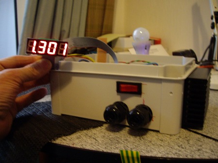
If the starting point is set to 65500, which is interpreted as 65.50 kWh, the display soon rolls over and starts again from 0.
This is because the maximum value of an unsigned int is 65535.
An alternative way of exercising the 4-digit display is to use segCheck_bothDisplays.ino. This sketch runs through each possible value in each location. Before gluing a display module into an enclosure, I run this sketch to make sure that none of its segments have failed. As with the previous sketch, the #define PIN_SAVING_HARDWARE line needs to be included or commented out depending on which version of the hardware is in use.
Here are two possible problems that can occur with the display:
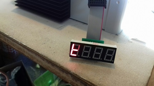
// #define PIN_SAVING_HARDWARE
otherwise the display will probably look like a small letter "t"
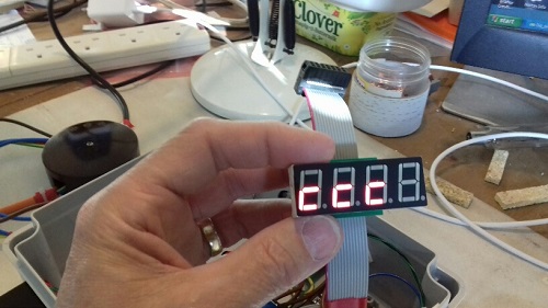
Instead of "0.000", it will show this "ccc " image.
This problem can be solved by removing the plastic lug on one of the ribbon cable connectors so the cable can then be reversed.
Testing the output board.
The primary purpose of the Router is to control the supply of mains power to the load. This switching operation is performed by the triac which forms part of the output board.
The output board may have already been tested in isolation. Now that a working main board is available too, the output board can be re-tested in-situ using a test sketch which drives the relevant control pin up and down. For this purpose, temporary 3-core cables should be fitted for the mains supply and load connections.
Here is a suitably modified version of the standard example sketch, blink.ino, in which the control pin has been changed to digital IO pin 4. DIO4 drives one of the pins at the "trigger" connector, the other pin is 3.3 V. For compatability with previous hardware, the triac becomes active when port DIO4 is driven low.
Once blink_dig4.ino has been uploaded to the processor, the output load will hopefully cycle on and off as intended. If it's not behaving in this way, it will be necessary to pause and check everything carefully. If individual tests for the main board and output board pass, then this combined test should work too, assuming that the low-voltage control cable that runs between them is in place and correctly orientated (i.e. '+' to '+').
If the output board does not appear to be working, correct operation of the main board can be easily verified using an LED and series resistor at the "trigger" connector.
Compliance with standard electrical tests
If the DPST mains switch is set to 'off', the processor will stop running (because its DC supply has been lost) but the override switch will continue to function. This is the mode in which the installation should be verified by an electrician: mains switch 'off', override switch 'on'.
Any kind of mains indicator is likely to interfere with (or become damaged by) the standard electrical test of Insulation Resistance, hence the need to disconnect them for testing purposes. This principle is shown in the next pair of photos:
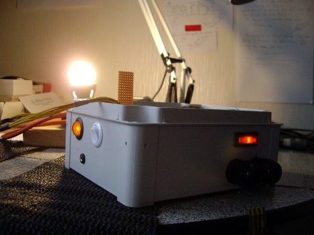
The red illumination within the override switch is visible because its Neutral supply - as supplied by the mains switch - is present.
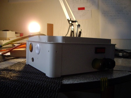
The override switch no longer has its Neutral supply. So, although it still functions mechanically as before (the load remains on), the illumination is no longer operational.
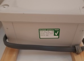
Ability to divert surplus power (or "Balance Test")
By this stage of the Build Sequence, each of the main components should have been tested in some way. The operation of the voltage and current sensors is covered within the section for the main board. The display and output boards have already been checked within this section.
[Satisfactory results from the RawSamplesTool, as described in the Main Board section, indicate that the voltage and current sensors are working properly. Running the calibration sketch, as described in the Calibration and Installation section, is another way of checking that all is well with the measurement side. It is well worth confirming that the input stages are OK before moving on to test the complete system as a single unit.]
Now it's time to see whether everything will work together as a complete system. Before wiring the Router into a 'live' power-generating environment, it may be helpful to simulate some surplus power within a test rig.
NB. Calibration is described on the Calibration & Installation page. For a 3.3V system usinmg standard components, powerCal is likely to be around 0.045. Setting powerCal_grid and powerCal_diverted to this figure should be fine for the offline checks in the rest of this section. These two variables are part of the MK2 PV Router sketch. For 5V systems, the powerCal values will be approx 50% larger.
The job of the Mk2 Router is to maintain a balance between generation and consumption. To do this, it has to sense the energy flow in both circuits. In a real operating environment, only one cable needs to be monitored, at the grid connection point. But in a test environment where generation has to be simulated, CT1 needs to be clipped around two wires.
For convenience, I've posted an alternative sketch which allows a complete Mk2 rig to be very easily tested. This sketch includes 1kW of synthesized surplus power, so there's no need for a second circuit. After clipping CT1 around the appropriate core of the output circuit, precisely 1kW of power should be diverted to the output load. If the load is staying on permanently, that could be because the feedback is positive rather than negative. To fix this, the orientation of the CT can be reversed or the other core of the output cable can be used.
This sketch is: balanceCheck_1kW.ino
NB. For this sketch to run, the TimerOne library needs to be installed within the Arduino IDE. A zipped copy of this folder is available on the Downloads page.
A 'proper' test-rig for balance, with plenty of supporting information, is presented in Section 8 of my Diverting Surplus PV Power article. Although that article was written in the context of an Unduino Uno or emonTx, the principle of operation has not changed. An updated version of that diagram, as shown below, is available here.
A simple test rig for the Router.
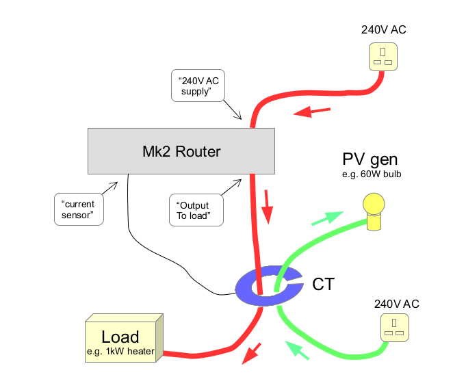
Only one core of each cable should pass through CT1. The red and green arrows are to show that the direction of energy flow is opposite in these two circuits.
Power to the load will be regulated by the Router in such a way that the net flow of current through CT1 is zero.
Assembling a test-rig of this type is not as difficult as it may sound. Having temporarily equipped my completed router with a 13A plug and socket, its feed and load circuits are already 'live'. Now I just need another cable to supply whatever appliance will be used to simulate my PV. A simple extension lead with its cores exposed for a short section is all that is required …
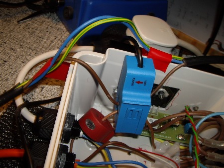
CT1 (blue) needs to be clipped around one core of each circuit, i.e. the generation circuit from above, and the load circuit from below.
CT2 (red) just monitors the diverted power, so is only located around one core of the load circuit (white flex).
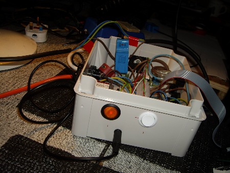
NB. The two wires that run through CT1 need to have their current flowing in opposite directions. This is easy enough to check. From the Line side of each circuit, just follow the electrical path until the CT is reached. You need to 'arrive' at CT1 from opposite directions.
In the photo above, the Line (brown) feed in my 'generation' cable arrives at CT1 from the left. The current for my dump load goes via the output board and then passes through the CT on its way to the output gland, so here the current is flowing from right to left. The two currents are therefore flowing in opposite directions through the CT, which is correct.
Now we need to run a Mk2 PV Router sketch which can identify and divert surplus power. Various versions that run on this new hardware are available via the Downloads page. The simplest of these is:
NB. For this sketch to run, the TimerOne library needs to be installed within the Arduino IDE. A zipped copy of this folder is available on the Downloads page. Although this "version 1" sketch is fine for test purposes, I would always recommend using the latest version from the Downloads page for the final installation.
Having saved and uploaded this sketch, the display should start up in its "walking dots" idle mode. As soon as power is drawn via the black "PV generation" cable, the system should spring into life and a matching amount of energy will be diverted to the load. The display shows the total amount of energy that has been diverted since start-up. It will reset automatically after a pre-set period during which no surplus energy has been detected (the default period is 8 hours).
NB. In latitudes when days are substantially longer during the Summer months, the reset period may need to be reduced to ensure that each day's total is cleared before the next solar day commences.
If the display is not working, make sure that the #define PIN_SAVING_HARDWARE line is correctly configured. This aspect is described higher up this page in the "Testing the 4-digit display" section.
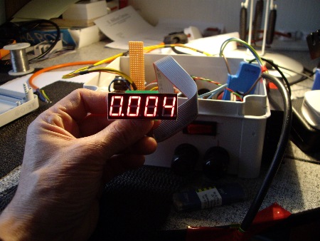
The output mode is dependent on the state of the mode switch.
If this switch is open, or not fitted, the system will be in normal mode; otherwise, it will be in anti-flicker mode.
If this behaviour is not seen, it probably means that the one or both of the CT's signals are reversed. This can be easily remedied by reversing the orientation of the CT1 or CT2 connectors. If CT1 is the wrong way around, the display will never leave its idle pattern. And if CT2 is the wrong way around, the displayed value will never increase. When they are both correct, the behaviour should be as described above.
NB. The rating of the load needs to be greater than the simulated PV, otherwise the system will not be able to maintain a balance between 'import' and 'export'.
The balance test, as described above, is as close as it's possible to get to a real 'live' environment. Once this test is operational, it's worth spending a few minutes to check that everything is behaving as expected. This is the ideal situation in which to put the system through its paces.
- can the operating mode be switched between "normal" and AF?
- does the display show the total amount of diverted energy (albeit uncalibrated)?
- do different levels of simulated power have the expected effect?
- does all activity cease when no simulated power is applied?
Normal and Anti-flicker settings are described in the technical background article that is referenced on the About page. A video showing an installed Mk2 PV Router operating in each of these modes can be found near the end of the calibration & Installation page.
Before moving on to the calibration and installation stages, it's worth checking that everything within the enclosure is as intended. Are all the screws tight, and does any of the wiring need to be tidied away? Has the heatsink been earthed? Is the external wiring area clear of obstructions, and are the mounting holes clear? Is there space for the internal CT, if it has not already been fitted, and the ribbon cable? And so on …