The 3-phase version
The prime task of the standard (single-phase) router is to monitor the energy flow to and from the premises. Any surplus energy is sent to a suitable load so that the rate of power consumption always matches the rate of generation. By staying within the penalty-free zone which most meters provide, no costs or penalties are applied while surplus power is being diverted.
The same principle is equally applicable to the 3-phase situation. In the UK, the user is charged according to their net consumption across all three phases. To operate in this way, the 3-phase Router needs to monitor the energy flow on each of the phases separately, and then add these individual values together. Once the net flow is known, any surplus energy can be diverted in a similar way as for the single-phase situation.
Since June 2014, a 3-phase Router of my design has been working satisfactorily at a premises where PV is available on all three phases. The hardware platform for that project was a one-off construction, but I have since commissioned a 3-phase PCB for this purpose. This PCB layout has been recently revised as noted at the end of this page. Circuit diagrams for both versions are available via the Downloads page.
For use in the USA:
The 3-phase version is well suited to any 1-phase environment where there are twin 'hot' feeds, such as in the United States. By measuring the Voltage and Current for each half of the supply separately, the total amount of real power can be accurately calculated. When using this approach, only two of the three pairs of V & I sensors would need to be populated.
However, because utility meters in the US only measure the 240V L1-L2 voltage, it makes sense for a diverter of surplus power to do likewise. My 1-phase PCB can therefore provide sufficient capability for such applications. Two measurements of current are required, each of which is associated with one-half of the measured voltage. Software for a split-rail application is available on request.
Two of my original 3-phase PCBs are shown in a built-up state in the photo below:
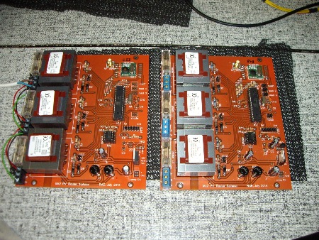
These two boards have been assembled in slightly different ways. The one on the left operates at 3.3V. Up to three (triac-based) output stages can be used with this configuration.
The board on the right has a 5V regulator, so the whole of the board (apart from the RF stage) operates at this higher voltage. Running this board at 5V rather than 3.3V has two advantages:
- The combination of the 16 MHz clock rate and the processor's supply voltage now lies within the specification of the Atmega 328P, rather than being slightly outside it;
- One or more SSRs can be used as the output stages without requiring any extra components.
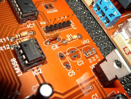
If the RF facility is to be used with the 5V version, an additional step-down regulator (VR2) is required to provide 3.3V to the RFM12B. The difference between these two versions is described in more detail later.
Performance
A 3-phase power monitor should display minimal crosstalk between the three channels and have minimal background drift. Both of the above boards have been tested on the bench and found to have good performance in these areas.
Voltage and current waveforms (at Vcc = 5V):
Background power and crosstalk data (at Vcc = 3.3V):
For this layout, the analogue and digital supplies for the processor have been kept separate, and the sensitive signals from the input sensors have been shielded. These simple measures appear to have resulted in a board that is well suited for its intended purpose.
Housing the PCB
With the 3-phase PCB being 50% larger that the standard one, and more external connections being required, it is less obvious how this new board should be assembled into a complete system. One possible approach would be to mount the main board within an enclosure of its own, and for each output stage to have its own separate enclosure.
When used on its own, this new PCB could provide a compact means of monitoring a 3-phase supply. It will just fit inside the size of enclosure that is featured on the preceeding pages.
Another possible arrangement would be to have a larger enclosure in which two output stages are mounted alongside the main board. This may be an attractive configuration for many users. I have therefore built up such a system which is now described in more detail.
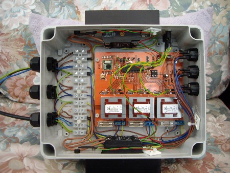
Output stages are present for L1 and L3, but not for L2.
All power connections are at the top (left).
At the bottom (right), there is a double-pole mains switch for each of the phases.
Although my standard output board will work satisfactorily in a 3-phase environment, this unit has been equipped with a pair of Solid State Relays instead. These are from a reputable manufacturer, and bear the CE mark of approval. This may be an important factor for some users, or their electricians.
The Crydom D2425 product appears to be well manufactured and performs well. Cheaper SSRs are available, but I would not recommend using them.
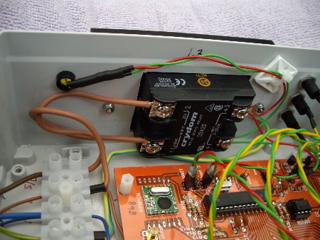
The SSR is held to the heatsink by self-tapping screws. The earthing lead is attached at one of these points.
An LED (with series resistor) shows when the output is 'on'.
To ensure that an SSR is controlled reliably, the processor needs to be operated at 5V. This is easily achieved by using a 5V voltage regulator rather than the usual 3.3V equivalent. If the RF facility is also to be used, an additional step-down stage is required as shown in the photo below:
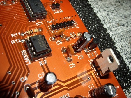
(these components are absent in the next photo)
In this case, the extra voltage regulator is not required. Power can be provided to the RFM12B using a simple wire link at VR2.
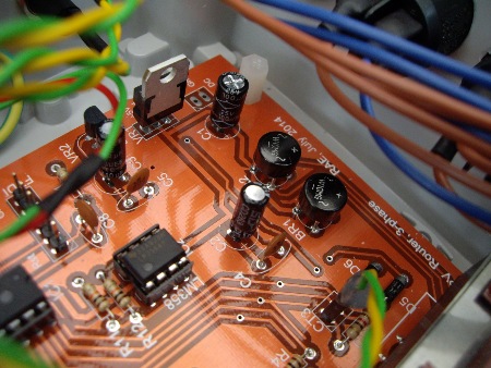
This requires the use of six diodes rather than the usual four, hence there are two bridge rectifiers on this board rather than just one.
The benefits of 3-phase rectification are explained here (bottom of the page)
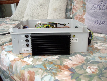
The jack-sockets for all three CTs are on this side too.
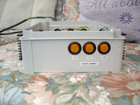
The bottom of the enclosure has a double-pole mains switch for each of the phases.
Each of these switches supplies power to the associated transformer on the PCB.
As with the 1-phase version, power for the output stages does not pass through these switches.
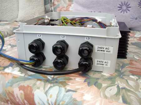
The top of the enclosure houses the glands for all the input and output cables.
For test purposes, only one input and one output have been connected.
For this unit, which only has output stages for L1 and L3, there is no need for the central gland on the upper row.
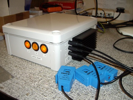
The CTs need to be clipped around around the three incomers. The CT cables can be extended for several metres without affecting the system's performance.
In normal operation, all three mains switches would be in the 'on' state.
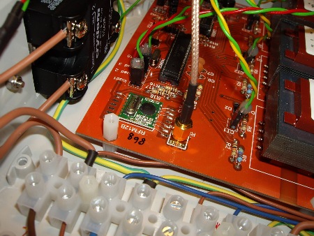
This extender cable screws directly to the receptacle on the PCB.
The fitting of the RFM12B module can be seen in detail here
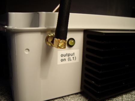
The other end of the aerial cable can be fixed to any convenient point on the enclosure.
The aerial should be chosen to match the frequency of the RFM12B.
RF aerials with SMA fittings are available in various forms. This is a 1/4-wave right-angled aerial for 868 MHz operation.
∗ ∗ ∗
With the enclosure shown above, only one output stage can be mounted on either side. If more output stages are needed, a larger enclosure could be used along with larger heatsink. The photo below shows a Schneider NSYTBS292412 ABS enclosure together with a 220 mm length of profile 333AB heatsink from ABL Components.
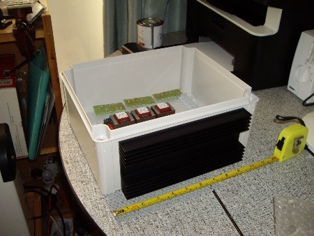
In free air, this heatsink has a stated thermal rating of 1.035 degrees C / Watt.
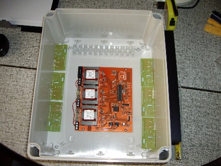
With the larger enclosure, there is space for up to six output stages, either triac-based or SSRs.
If the RF facility is not required, up to six output stages could be independently controlled by this PCB.
For a finer degree of control, a 3-phase water heater could be treated as three separate loads.
Upgrade to Rev 2 (2015)
Various changes have been made as shown in the photo below:
- - all digital ports are tracked to easily accessible points.
- - ports D3-D9 can be individually associated with either Vcc or 0V power pins;
- - protection has been improved by adding a series resistor to each of the CT inputs;
- - the Vref circuit can be operated either at Vcc or using the processor's internal 1.1 Volt reference.
- - there is now provision for a reset button/switch;
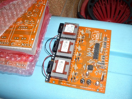
The red link, marked L1, is to configure the reference circuit to operate at Vcc. If L2 and L3 were fitted instead of L1, the internal 1.1 Volt reference would be used.
A circuit diagram for this latest 3-phase PCB is available in the "Diagrams & Guides" section of the Downloads page.
Parts list for the 3-phase PCB:
| Identity on PCB | component description | # used | notes |
|---|---|---|---|
| (none) | 3-phase PCB, Rev 2 | 1 | |
| TXFR1-TXFR3 | transformer 2 x 6V | 3 | 835-401, JPR Electronics |
| (none) | fuse (100mA), slow blow | 3 | 20 x 5 mm |
| 100mA fuse | fuseholder | 3 | for FS1-FS3 |
| TB1-TB3 | T/block, 3-way, 90-degrees | 3 | |
| Atmega 328P | processor, Atmega 328P | 1 | |
| IC1 | DIL socket, 28-pin | 1 | for IC1 |
| LM358 | op amp, LM358 | 1 | |
| IC2 | DIL socket, 8-pin | 1 | for IC2 |
| BR1, BR2 | bridge rectifier | 2 | |
| VR1 | 5V voltage regulator, TO-220 | 1 | |
| X1 | crystal, 16 MHz | 1 | |
| D1-D6 | diode, 1N4007 | 6 | |
| C1 | capacitor, 100 uF electrolytic | 1 | |
| C2 | capacitor, 10 uF electrolytic | 1 | |
| C4, C6-C8 | capacitor, 100 nF ceramic | 4 | |
| C9, C10 | capacitor, 22 pF ceramic | 2 | |
| R1 | 0.25 Watt resistor, 47K | 1 | |
| R2-R4 | 0.25 Watt resistor, 180R | 3 | extra loading, see Note 2 below |
| R5-R7 | 0.5 Watt resistor, 1K0 | 3 | extra loading, see Note 2 below |
| R8-R10 | 0.5 Watt resistor, 150R | 3 | or a lower value for datalogging |
| R11, R12 | 0.25 Watt resistor, 10K | 2 | |
| R19-R21 | 0.25 Watt resistor, 1K | 3 | |
| R22 | 0.25 Watt resistor, 1M0 | 1 | or 100K, see Note 1 below |
| various | SIL pin strip (0.1" spacings) | 18 (typ) | for FTDI, CTs, reset & IO ports |
| various | SIL socket, 2-way | 7 (typ) | for CTs and IO port connections |
| various | SIL socket, 3-way | 2 (max) | for L1-L3, or use soldered links |
| for an RF-equipped board: | |||
| RFM12B | RFM12B, 433 or 868 MHz | 1 | |
| RF aerial | SMA receptacle | 1 | |
| VR2 | 3.3V regulator, small (TO-92) | 1 | |
| C3 | capacitor, 10 uF electrolytic | 1 | |
| C5 | capacitor, 100nF ceramic | 1 | |
| R13-R15 | 0.25 Watt resistor, 4K7 | 3 | |
| R16-R18 | 0.25 Watt resistor, 10K | 3 |
Note 1:
The value for R22 is shown on the circuit diagram as 100K. That value is OK when the unit is free standing, but the reset process may not work reliably when a USB programmer is connected. A 'weaker' pullup is therefore recommended, hence the value of 1M0 in the above table.
Note 2:
The values for R2 - R4 and R5 - R7 are each one hundredth of those shown on the circuit diagram. This is to provide some loading for the transformer which can prevent it from going into saturation. This topic is discussed in more detail on the Technical Notes page.
Upgrade to Rev 3 (2022)
Changes from the Rev 2 version include:
- - the transformers are now Myrra 44163 or equivalent, as for the Rev 4.1 single-phase PCB;
- - the N and PE connections for the 3-phases can be linked on the board;
- - the unused half of IC2 is tied to ground rather than floating;
- - test pads are available for all of the power rails;
- - the reference voltage for the Vref circuit is no longer selectable (because the 1.1 Volt option was never used);
- - a 0V connection has been added alongside each of the five digital IO ports that are associated with the RF module;
- - the logo for the RF module has been modified to convey the correct orientation of that component more reliably;
- - the diameter of the mounting holes has been increased to 4mm.
- - the colour of the board is now cherry red rather than orange.
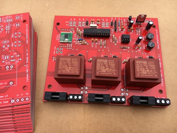
As with previous versions, VR2 provides a reduced voltage supply for a 3.3V RF module.
Using the 3-phase control board
Software to run on this board is available via the Downloads page. My 3-phase Router sketch supports multiple loads with the ability to change the priority order using an external switch.
The standard software is for use with a 3-phase meter that registers the net consumption of energy, as in the UK. In other locations such as Finland, the consumption on each phase is monitored and charged for separately. To work correctly alongside such a meter, the 3-phase control board must operate as three separate 1-phase Mk2 units, one on each phase. That alternative software version is available on request.
Datalogging via RF of the average power and RMS voltage for each phase is supported. The format of the transmitted data is directly compatible with the Open Energy Monitor's emonCMS system. The 3-phase PCB can also be used for monitoring only; there is no need for on-site generation to be present.