Building & Testing the output PCB
A Solid State Relay (SSR) can also be used as an output stage. Details about that option can be found on the 3-phase page.
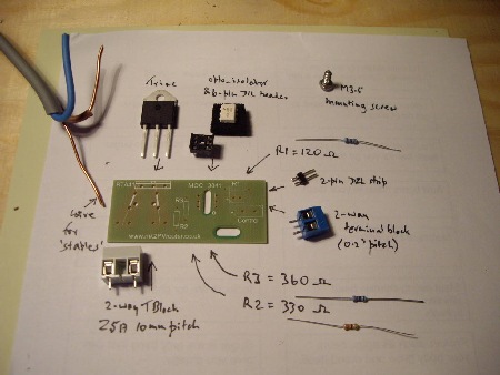
Here is a complete set of components for the output PCB:
Here is a circuit diagram for this board:
The first stage of the assembly process is to fit a pair of solid copper 'staples' which increase the ability of the board to carry high currents. The recommended cross-sectional area is 1.5 mm², as is generally found for the earth core in 2.5² T&E cable.
Notes:
The latest batch of these PCBs have some minor improvements but are assembled in a similar way and have identical performance. There are some photos at the end of this page.
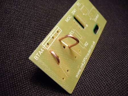
First, the wire is bent into a suitable shape for fitting through these holes …
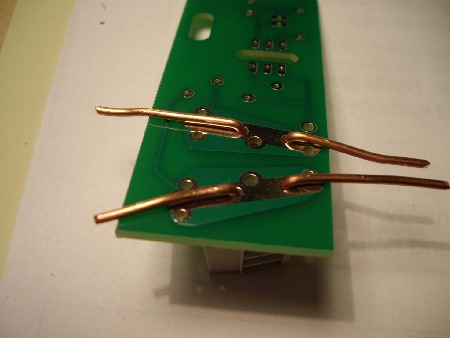
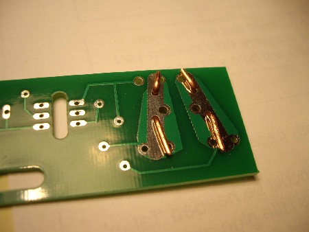
With the copper staples in place, all of the low-power components can now be fitted. As shown on the circuit diagram:
R1 = 120 ohms (when running from a 3.3V source, or 180R for 5V operation)
R2 = 330 ohms (the lower-left one of the pair)
R3 = 360 ohms (the upper-right one of the pair)
If fitting a DIL header for the opto-isolator or "trigger" IC, the notch should be at the bottom alongside the circle on the PCB. These features both indicate pin 1.
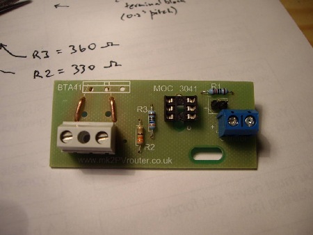
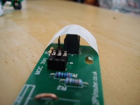
The low voltage pair of wires for controlling the triac can be connected in two ways. The conventional approach is to use a standard screw-terminal block with 0.2" pitch. An alternative approach is to use a 2-pin length of 0.1" pitch SIL pin-strip. By means of a corresponding SIL socket, the control cable can then just be pushed home after everything else is in place. Simple and effective, and no need for any tools.
In the photo above, the large grey connector for the power wiring is shown in its correct position but has not yet been soldered into place. The fitting of this component is described later.
When fitting the small 2-way terminal block for the control cable, care must be taken not to strain the delicate PCB tracks. On one occasion, I found that I had broken one of these tracks as shown in the photo below.
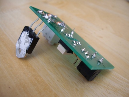
I have most likely twisted the component to achieve proper alignment without fully re-melting the solder.
The same technique is useful for attaching the SMA receptacle for the aerial.
For terminating the high-current cables, there are three options:
- a 25A Terminal Block with 10mm pitch;
- a pair of standard 2-pin Terminal Blocks of 0.2" pitch, with one cable in each;
- pass each cable through the board and solder it directly to the copper 'staple'.
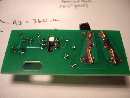
This component can be temporarily held in place by bending the copper staples so that they just nip against the protruding pins.
Then, with a nice hot iron…
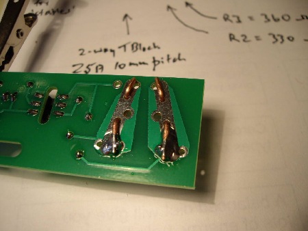
Before testing an output board, the triac must be added. When building a complete system, it may be best to wait until the triac's mechanical fit to the heatsink has been determined. The triac can then be confidently soldered into place before the output stage is tested.
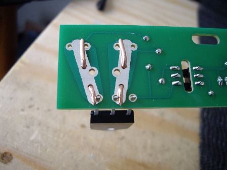
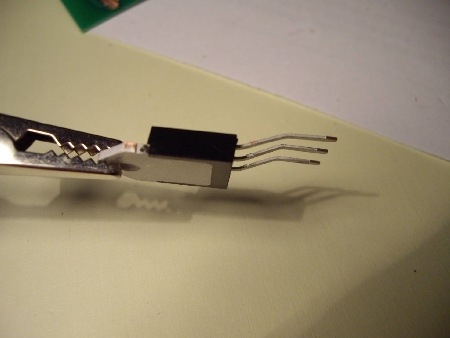
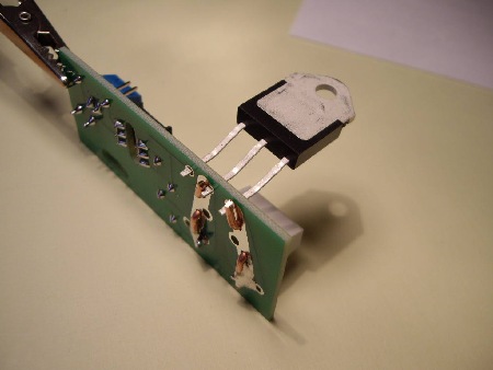
By lowering the heatsink slightly, the triac's leads will not need to be quite so long.
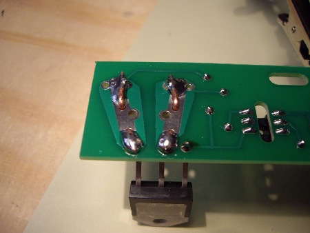
…then all three legs can be soldered firmly into place.
For the A1 and A2 connections, a good hot iron and plenty of solder are required.
When soldering the centre pin (A2) in place, make sure that the solder does not bulge out towards the gate pin. If it does, some solder should be carefully trimmed away. It appears that I was rather heavy-handed with the solder above.
With the triac firmly in place, the board is nearly ready to be tested. The final stage is to insert the opto-isolator or trigger chip.
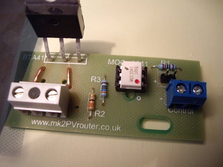
The dot on the chip (highlighted here in red) needs to be alongside the circle on the PCB.
If fitted the wrong way round, it won't work. But thanks to the layout of its pins, it should survive the experience.
When building an entire system, it may be more appropriate for the completed output stage to be mounted into the enclosure before being tested. The guidance below is offered for when an output stage is to be tested in isolation.
Safety Warning:
To test that the trigger & triac are working, access to 230V AC mains voltage is required.
Please take great care, and do not undertake this next stage unless you are competent to do so.
For my own purposes, I have constructed a rig which allows me to test output boards with or without the triac being soldered into place. That rig is shown at the top of the Photo Gallery page. When testing an output board, it is important that the triac forms part of the electrical circuit, otherwise all of the load current will go via the opto-isolator circuit and something will rapidly expire.
With due regard for the above Safety Warning, the simple approach that I've used below should be fine for testing individual boards. Here is a schematic diagram for this operation:
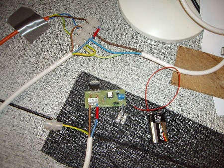
My test load plugs into a 13A socket on the orange cable just off the picture.
The duck tape is to prevent everything sliding off the table when a test load is plugged in!
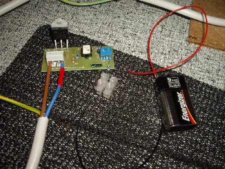
To activate the circuit, I just touch the red wire onto the +ve control input at the terminal block.
The triac will be OK for a few seconds without a heatsink.
Update, October 2015:
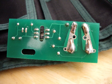
The latest batch of these boards includes some minor improvements:
- - The spacing of the holes for the triac is now correct at 5.5mm; previously, it was 5mm.
- - The labelling of R2 and R3 has been changed to remove any ambiguity.
- - The solderable area around the wire 'staples' has been slightly changed.
- - The upper surface now has a solder-resist layer.
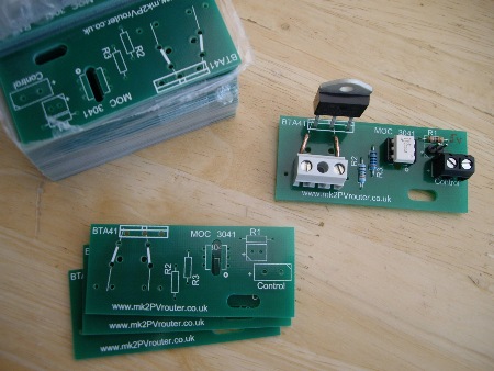
The solder-resist layer allows the silk-screen image to be seen more clearly.
Dual-output version (max 3kW) - introduced August 2017
A dual version of the output stage PCB is now available. This allows the triacs for two independent loads to share the same heatsink. This arrangement is suitable for a two-load system where surplus power will not exceed ~3 kW.
Update Summer 2021
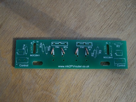
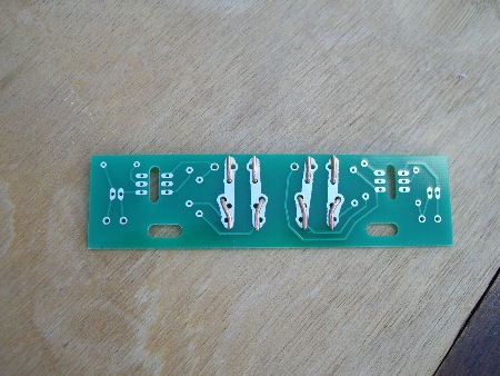
The dual version of the output stage PCB has been reworked as shown below. It now has two layers of copper which makes the tracks more robust. The hole locations for the 1.5 mm² solid copper 'staples' have been adjusted and there is no longer any doubt as to where they should be fitted.
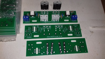
Care must be taken to fit the components in their correct locations.
As shown on the PCB and by the red dots in this photo, IC1 and IC1a are opposite ways around.
NB. With the earlier single-sided version, each 1.5 mm² copper 'staple' should be threaded through the larger of the two holes near the middle of the board. This arangement is shown in the next two photos. Otherwise there may not sufficient clearance for the power connectors.
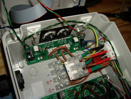
To provide enough power terminations for two loads, a second connector block has been mounted above the first one.
NB. The element that's next to the Earth on the lower connector should be labelled "N" not "L".
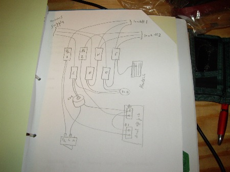
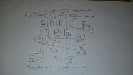
At the time when this box was built, CT2 was fitted around the two Line wires rather than the Switched-Line ones.
That arrangement was necessary because the YHDC TA17L-04 CT at that time had a small central aperture which could only accommodate two 1.5mm² wires.
With this version of the power wiring, one of the power connectors of the dual output stage PCB had to terminate two 1.5mm² wires which was a tight fit.
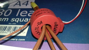
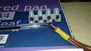
This connection can be achieved by stripping the ends of the four wires, and taping then tightly together BEFORE their exposed copper strands are twisted into a single bundle.
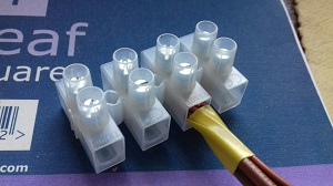
Make sure that the screw and tongue of the connector element are fully retracted first.
The 2 x 3kW version
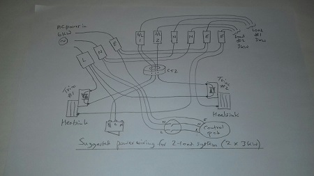
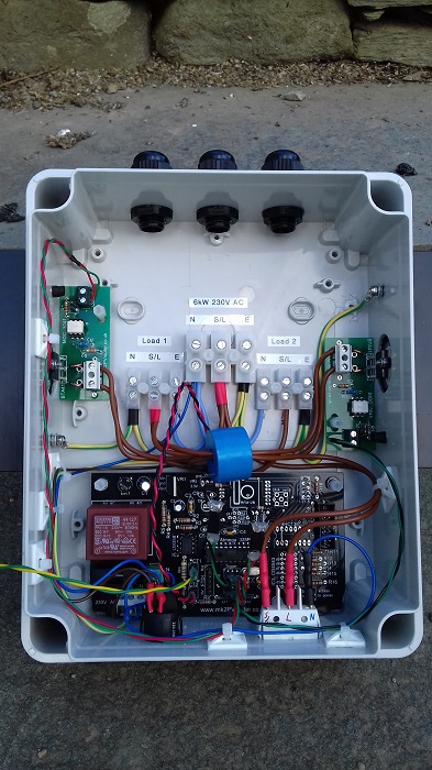
This system uses the Rev 4.1 control board and a 2VA Myrra 44127 transformer.
To optimise the performance, an extra resistor has been included in the control cable for each output stage. This upgrade is described in the "transformer compensation" section of the Technical Notes page.
When I saw a photo, I advised that heatsinks should always be mounted vertically where air circulation is unrestricted rather than on the top or bottom surfaces. The layout was duly changed and I regard the final outcome as being excellent.
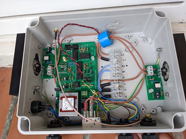
The unwanted hole at the top has been very effectively filled by the disc that was carved out for the new hole at the side.
A similar 2 x 3kW system in "landscape" mode can be seen near the end of the Photo Gallery.
Parts list for the output stage PCB:
| Identity on PCB | component description | # used | notes |
|---|---|---|---|
| output stage PCB | 1 | single or double | |
| mounting screw | 1 | m3.5, 8mm, pan head | |
| BTA41 | BTA41 600V triac | 1 | |
| MOC 3041 | opto-isolator | 1 | zero-crossing, not the direct acting type |
| DIL socket, 6-way | 1 | for the opto-isolator IC | |
| R1 | 120R, 0.25W resistor | 1 | or 180R for 5V use |
| R2 | 330R, 0.25W resistor | 1 | |
| R3 | 360R, 0.25W resistor | 1 | |
| terminal block, 2-way, 25A | 1 | 10 mm pitch, for the power connections | |
| Control | terminal block, 2-way, 1A | 1 | 2.54 mm pitch, for the control cable |
| SIL pin strip (0.1", 2-way) | 1 | for a LED indicator assembly | |
| SIL socket, 2-way | 1 | for a LED indicator assembly | |
| 1.5mm^2 copper wire, 3" | 1 | copper "staples" to carry the load current |
