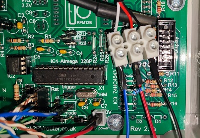
Main PCB - options for use of I/O ports
The Atmega 328 processor has a total of 20 IO ports. On this PCB, five of these ports are allocated for specific purposes: digital 0 & 1 are reserved for the Serial interface, and analog 3 - 5 are for the voltage and current sensors. The remaining 15 ports are available for general IO duties.
On the green (Rev 2) PCBs, access to each of these 15 IO ports is provided at a designated location on the PCB. In each instance, a nearby power connection is available. This is generally a ground pin, but for five of these ports the associated power connection can be selected to be either Ground or Vcc.
A complete list of these access points for the Rev2.1a PCB is given in the following table. Equivalent information is then presented in descriptive form. Finally, three PCBs are presented to illustrate different ways that these ports may be used in practice.
| IO port identity | Atmega pin # | Access point | power pin polarity | span to power pin & direction | normally used for | Notes |
|---|---|---|---|---|---|---|
| digital 2 | 4 | below Atmega pin 4 | Gnd | 0.1" below | RFM12B | |
| digital 3 | 5 | LH pin of "mode" port | Gnd | 0.1" to right | "mode" | |
| digital 4 | 6 | LH pin of "trigger" port | Vcc | 0.1" to right | "trigger" | |
| digital 5 | 11 | IC3 pin 7 | Vcc / Gnd | 0.1" to right | display | 1 |
| digital 6 | 12 | IC3 pin 5 | Vcc / Gnd | 0.1" to right | display | 1 |
| digital 7 | 13 | IC3 pin 4 | Vcc / Gnd | 0.1" to right | display | 1 |
| digital 8 | 14 | IC3 pin 3 | Vcc / Gnd | 0.1" to right | display | 1 |
| digital 9 | 15 | IC3 pin 2 | Vcc / Gnd | 0.1" to right | display | 1 |
| digital 10 | 16 | middle of R23 | Gnd | 0.1" to left | RFM12B | 2 |
| digital 11 | 17 | middle of R22 | Gnd | 0.1" to left | RFM12B | 3 |
| digital 12 | 18 | top of RFM12B area | Gnd | 0.1" to left | RFM12B | |
| digital 13 | 19 | middle of R21 | Gnd | 0.1" to left | RFM12B | 4 |
| an 0 (dig 14) | 23 | LH end of R11 | Gnd | 0.2" above | display | |
| an 1 (dig 15) | 24 | IC4 pin 1 | Vcc | 0.3" above | display | |
| an 2 (dig 16) | 25 | IC4 pin 2 | Gnd | 0.1" to right | display |
Notes:
- Selection of the associated power pin is made by means of a wire link at IC3. For Vcc, a 0.2" link is required at pin 16. For Gnd, a 0.1" link is required at pin 8. Only one of these links must be present to avoid the power rails being shorted together. This selection applies to all of D5 - D9.
- For access to D10, a 0.4" wire link is required at the location of R26.
- For access to D11, a 0.4" wire link is required at the location of R25.
- For access to D13, a 0.4" wire link is required at the location of R24.
In the photo below, a Rev 2.1 PCB has been equipped with an LED at each of the 15 locations where these IO ports can be accessed.
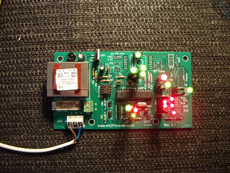
In places where the associated power pin can only be ground, a green LED has been used.
In this Video clip , ports 2 - 16 are operated in sequence.
(apologies for the sound track!)
∗ ∗ ∗
The "port locations" where IO ports can be accessed fall into three main areas. Each of these areas (or zones) is now described in more detail.
The first of these areas (Zone 1) makes use of the connection points for IC3 & IC4 when the 4-digit display is not in use. IC3 provides five "port locations" where the associated power pins can be connected either to ground or to the positive power rail. This selection requires a short wire link to be fitted at either pin 8 or pin 16 respectively.
IC4 provides three "port locations" where the associated power pins are fixed. Pin 1 of IC4 can be easily used with the positive pin which is directly opposite (at pin 16 of the same IC). Pin 2 of IC4 can be easily used with the adjacent ground pin (at pin 3). Pin 8 of IC4 provides a convenient ground pin for the left-hand end of R11 where the Analog 0 port may be accessed.
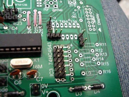
Access to 8 "port locations" is provided in the IC3 & IC4 area.
For this board, the associated power pins at IC3 have been configured to be Vcc rather than ground (the wire link at pin 16).
These access points are only available when the 4-digit display is not in use.
The second area of interest (Zone 2) is in the vicinity of the RFM12B module. This area provides access to four of the five IO ports that can be used for other purposes when the RF module is not present. For each of these points, the associated power pin is ground.
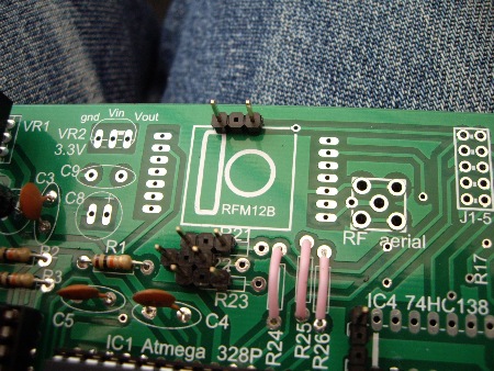
To use the access points at R21 - R23, wire links must be fitted at the associated R24 - R26 locations.
Here, all three of these points are in use, so links have been fitted at each of these locations.
The access point at the top of the RFM12B area does not require an extra link to be fitted.
NB. The above photo shows a Rev 2.1 board in which the spacings of these pins is 0.2". For Rev 2.1a, these spacings have been reduced to 0.1"
The final area of interest (Zone 3) lies between the crystal and the FTDI connector from where the processor is programmed. Immediately to the right of the FTDI connector is where digital 2 can be accessed. This is the fifth of the digital pins that can be used for other purposes when the RFM12B module is not present. Its associated power pin is ground.
To the right again is where the final pair of IO ports can be accessed. These locations are labelled "trigger" and "mode". The "trigger" port is normally used to control a triac with an active-low signal, so the associated power pin is positive. The "mode" port is normally used to sense the state of a passive external switch. Because each IO port of the the Atmega processor has a (selectable) internal pull-up resistor, the associated power pin in this case is ground.
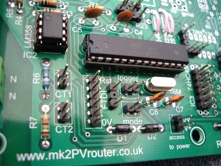
For a Mk2 PV Router application, the "trigger" and "mode" ports are normally used for dedicated purposes.
These two ports can also be used in other ways, hence their inclusion here.
Access to port D2 (Atmega pin 4) is also available here.
NB. The above photo shows a Rev 2.1 board. For Rev 2.1a, the spacing for access to port D2 has been reduced from 0.2" to 0.1". This access point is directly below pin 4 of the processor.
∗ ∗ ∗
As mentioned earlier, these IO ports can only be used for other purposes when they are not required for their normal roles. This is generally to support the 4-digit display and/or the RFM12B module. To free-up some IO pins for other purposes, either the RF facility or the display will have to be omitted.
In order to verify the performance of the Rev 2.1 layout, I assembled three of these PCBs in different ways. The basic Mk2 PV Router operation is supported by all versions (including the "trigger" and "mode" ports), but the remaining 13 IO ports are used differently in each case.
Board No 1: Display only (without pin-saving hardware)
When the pin-saving hardware is not in use, the 4-digit display uses 12 of the 13 available IO pins. The Main PCB page of the Build Guide explains that 14 links have to be fitted when the display is used in this way (the following photo is also shown there).
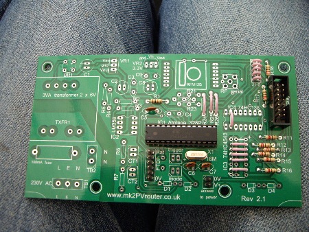
When the 4-digit display is set up in this way, the only "spare" IO pin is A1 at IC4 pin1.
For ease of testing this board, a DC supply was provided via the "access to power" connection.
Board No 2: Display and RF, with single-voltage operation (3.3V)
When only one voltage regulator is in use (i.e. VR1 = 3.3 volts), the VR2 regulator must be bypassed with a wire link.
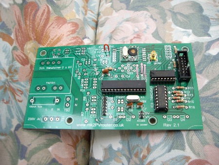
The link to bypass VR2 is shown in red.
When the processor is operating at 3.3V, wire links are required at the R24 - R26 locations.
The R21 - R23 locations must be left empty.
By fitting the pin-saving hardware, as shown above, the 4-digit display can be used alongside the RF facility. All of the IO pins would then be in use so none would be available for any other purpose.
Board No 3: RF, with twin-voltage operation
For this board, the voltage regulator VR1 is operating at 5V. This would be necessary if an SSR were to used for the ouput stage rather than a triac. Because 5V is higher than the RFM12B module can accept, a step-down stage is needed as shown in the photo below.
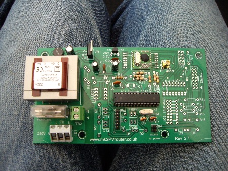
(Board 3)
Here, none of the "port locations" in the Zone 1 area are being used (at IC3, IC4 and R11).
The five such locations at IC3 could conveniently be used to drive a bank of SSRs.
Or the pin-saving hardware could be fitted to drive a 4-digit display.
The second voltage regulator and its associated components are described on the Main PCB Assembly & Test page.
∗ ∗ ∗
Temperature Sensor
From version 4 onwards, the sketch Mk2_RFdatalog_n.ino includes temperature sensing via the "mode" port. In the photo below, a Dallas DS18B20 sensor has been connected in this way.
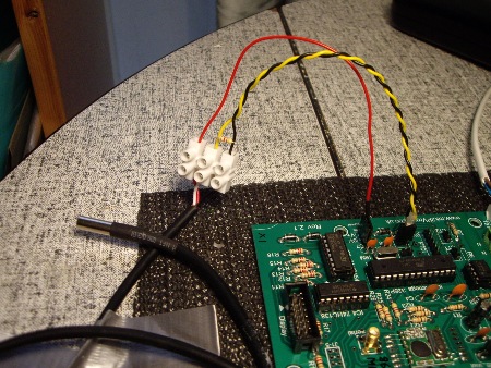
The Dallas sensor requires three connections: one IO port, ground, and the Vcc power rail.
Here, the "mode" port provides the first two of these connections, and Vcc is provided via the "access to power" port.
A 4K7 pullup resistor can be seen at the connector block. This resistor would need to be part of the external wiring.
When the 4-digit display and the RF module are both in use, the "mode" port is the only one that can be used for temperature sensing. But if either of those features is not required, the Dallas sensor can be moved to any IO port that is available. This may provide a tidier means of connection.
If the RF module is not in use, D10 can be used for the temperature sensor. The pullup resistor can then be housed on the PCB rather than having to be included in the external wiring. There is a photo of this arrangement on the Gallery Page.
If the 4-digit display is not in use, pins 2, 4 and 6 of IC4 can provide all three connections for the Dallas sensor, these being Analog 2 (D16), ground and Vcc respectively. With a bit of thought, it should not be too difficult to find somewhere for the pullup resistor to go …
