Building & Testing the main board
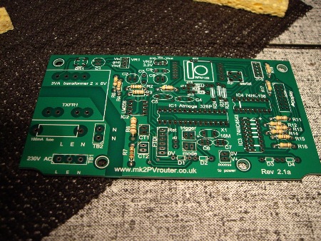
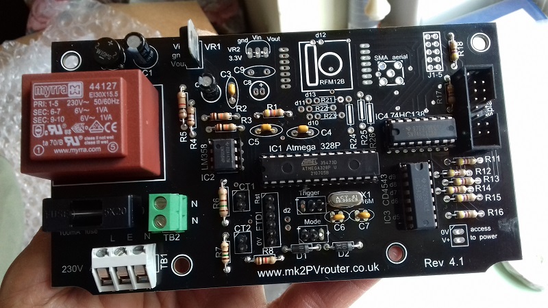
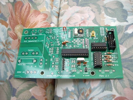
Four versions of this PCB have been produced of which the first three are shown below. While they all perform in a similar way, each version provides more flexibility than the previous one.
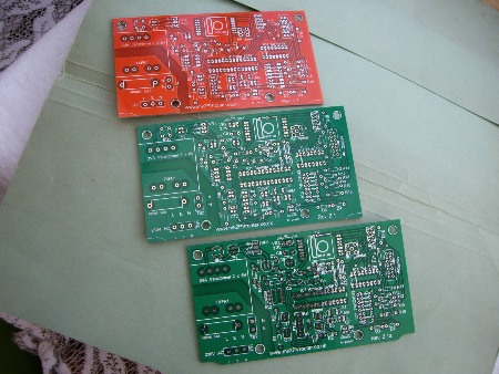
Rev 2.1 (green) has a separate power supply stage for the RF module. Easy access is provided to all IO ports.
Rev 2.1a (green) has pre-routed corners. Access to IO ports is with pin-pairs that have 0.1" spans wherever possible.
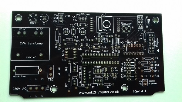
An extra resistor (R8) provides additional protection for the processor during times of high power consumption.
This assembly guide was originally written for the (orange) Rev 1.1 board, but I am gradually updating it to show the later PCBs. Where any significant differences exist between PCB versions, this will be noted in the text.
Before starting to assemble this board, I recommend looking through the whole of this page. Guidance about how the processor's many IO ports can be used can be found on the Main PCB - Port Options page.
Notes about programming:
To upload code (software) to this board, a programming facility which includes a programming adapter and a matching USB cable will be required.
Guidance about how to set up the standard programming facility for the Arduino platform is available at: https://www.arduino.cc/en/Guide/HomePage
Further detailed guidance can be found at openenergymonitor.org → Learn → Electricity Monitoring → Using the Arduino IDE;
then just follow the appropriate guidance for the Operating System you are using.
The programming facility for any Arduino-type hardware is known as the Integrated Development Environment (IDE).
Within the Arduino IDE, some adjustments may be required before new code can be uploaded:
- Tools→Board should be "Arduino/Genuino Uno".
- Tools→Programmer should be "AVRISP Mk11" (for any programmers that I supply).
- Tools→Port should match whichever new port appears when the programmer is connected to the host computer.
Programmer Types:
During the lifetime of this project, two different types of programmer have been available from my Shop.
Please note that these two programmer types require different USB cables and Device Drivers.
When used with MAC or Windows hosts, a Device Driver may need to be installed.
These two types of programmer are shown below, they being:
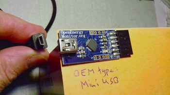
- OEM type (Open Energy Monitor)
- FTDI type (Future Technology Devices International)
(hi-res image)
the relevant Device Driver can be downloaded from:
https://www.silabs.com/products/development-tools/software/usb-to-uart-bridge-vcp-drivers
Please note that the 0V (ground) pin is at the TOP of the 6-way FTDI connector.
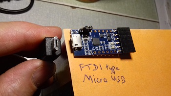
(hi-res image)
the relevant Device Driver can be downloaded from:
https://ftdichip.com/drivers/vcp-drivers/
(for Windows users, click on the "setup executable" link)
Please note that the 0V (ground) pin is at the BOTTOM of the 6-way FTDI connector.
The FTDI programmer includes a jumper which allows the voltage level to be selected between 3.3V and 5V.
When used with both 3.3V and 5V boards, I suggest that this jumper is left at the default (3.3V) setting.
If problems were to be experienced when programming a 5V board, it would then seem appropriate to try the higher voltage setting.
To see the results of Serial.print() statements, the baud rate of the Serial Monitor must match the
Serial.begin(<baud rate>) command in the sketch that is running. To open the Serial Monitor window,
click the "magnifying glass" icon on the main IDE screen. The baud rate can then be changed using the drop-down menu.
My software always operates at 9600 baud.
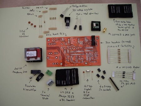
A complete set of components for the main board is shown in the photo below. A parts list and circuit diagrams are available via the Downloads page.
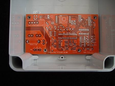
Later versions also have pre-routed corners. For earlier versions, the two lower corners had to be removed by hand as shown here.
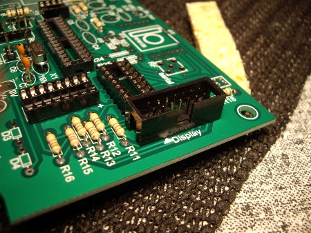
My preferred way of assembling this PCB is to fit the components in increasing order of height. In the photo below, all of the resistors that are necessary for the basic operation of the board and the display have been fitted. Only those which may be needed for the RF facilty have been omitted.
R6, which is the burden resistor for the primary current sensor, is rated at 1/2 Watt. This is to prevent possible overheating during periods of high consumption by the premises that are being monitored.
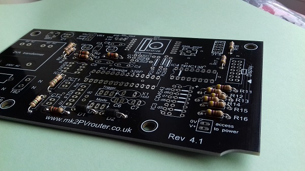
A wider spacing has been provided for R5 and R6 which are normally 1/2 Watt.
Diodes D3 and D3 have been removed, and the spacing for diodes D1 and D2 has been increased.
Resistor values are shown on the circuit diagram and are repeated here for convenience:
(please read the notes below which are relevant to these component values)
R1 = 47K. This provides the "pull-up" for the processor's reset line.
R2 = 10K. Along with R3, this provides a reference voltage for the input sensors.
R3 = 10K. Along with R2, this provides a reference voltage for the input sensors.
R4 = 100R or 180R. R4 & R5 reduce the size of the AC signal from the transformer.
R5 = 1K0. R4 & R5 reduce the size of the AC signal from the transformer.
R6 = 120R or 150R. This is the burden resistor for the 'grid' current sensor, which uses CT1
R7 = 120R or 150R. This is the burden resistor for the 'diverted' current sensor, which uses CT2
R8 = 1K0. This resistor is in series with CT1 to protect the processor from large signals (Rev 4.1 PCB only)
Notes about resistor values:
The original value for R1 of 10K, as used by similar monitoring systems, has been found to give unreliable performance with boards that are operated at 5V. The value of 47K lies within the specified range of 30K - 60K in the Atmel 328P datasheet (Rrst, on page 323 of 662) and is now recommended for use with all Mk2 boards.
As mentioned near the top of the Technical Notes page, lower values for R4 and R5 are now used to increase the load on the transformer. This can prevent it from going into saturation which distorts the output waveform. R4 = 100R is suitable for 3.3V operation. For best use of the ADC's input range, R4 should be increased to 180R for 5V operation.
The value for R6 and R7 was initially specified as 150R. When operating the processor at 3.3V, this gives a working range of ~4 kW. By reducing these values to 120R, the range is increased to ~5 kW. For a 5V system, the original value of 150R gives a working range of ~6 kW.
If whole-house datalogging is required, the working range of the 'grid' sensor can be increased by reducing the value of R6. However, it must be recognised that the sensitivity of the measurement system will be correspondingly reduced.
R6 = 56R will allow measurements of up to ~10 kW
R6 = 47R will allow measurements of up to ~12 kW
R6 = 39R will allow measurements of up to ~14 kW.
These burden resister values are for when the processor is operated at 3.3 V. If operated at 5V, these ranges are increased by approximately 50%.
R11 - R18 are the series resistors for the 4-digit display. If the board is to be operated at 3.3V, these eight resistors should be 220R. If operated as 5V, this value should be increased to 470R to maintain a similar level of brightness.
Next, the diodes can be added. These provide a degree of protection to the processor when high currents flow through the CTs. Although space is available for four protection diodes (two for each CT channel), only D1 and D2 are likely to be of any practical use. In most applications, the current that is measured by CT2 is relatively small so D3 and D4 can be safely omitted.
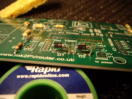
NB. These components must be fitted in the correct orientation as shown on the silk-screen layer.
Sections of 0.1" SIL pin-strip are used at several locations to provide low-power connections to the PCB. The FTDI header (from where the board is programmed) requires a 6-way section, and 2-way sections are used at various other locations as shown on the silk-screen image. Pin-strip can be cut to length with a sturdy knife or wire cutters.
I generally fit these SIL-strips at this stage because they can be difficult to adjust if nearby components are already in place. In the photo below, I am about to solder the 6-way FTDI strip into place.
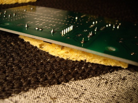
Non-vertical pin-strip can be easily corrected at this stage by re-melting the solder while gently pressing on the plastic part with a fingernail.
Don't forget to solder the rest of the pins into place too!
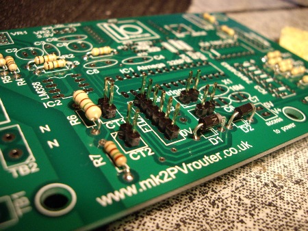
The "FTDI" port requires a 6-way section.
The "trigger", "mode", "CT1" and "CT2" connections each require a 2-way section.
With the Rev 4.1 PCB, the "trigger" and "mode" ports each have space for three pins rather than two. This allows those ports to be used in association with either of the power rails. For compatability with my published software, the "trigger" port (D4) will normally be used in active-low mode so only the right-hand pair of pins will be needed. And the "mode" port (D3) will normally be used in active-high mode so only the left-hand pair of pins will be needed. This arrangement is shown in the photo which follows.
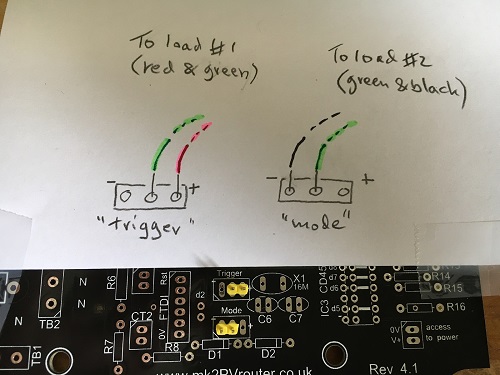
Note the locations of the 2-pin Single-In-Line strips at the "trigger" and "mode" ports.
The normal colours for wiring a 2-load system are also shown.
Next, I generally fit the header-sockets for the ICs. If the pin-saving hardware is in use, four ICs will be needed (IC1 - IC4); otherwise there will only be two (IC1 & IC2). This distinction is explained in more detail later.
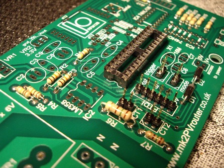
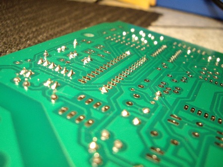
If any re-alignment of the component is required, it should be done before the remaining pins are attached.
The 4-digit display can be controlled in either of two ways. If the RF facility is not required, and those IO pins are not needed for any other purpose, a full set of IO pins on the processor can be dedicated to driving the display. This configuration requires the addition of fourteen wire links as shown in the silk-screen layer. The board in the next photo is being assembled in this way:
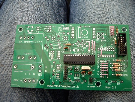
5 links at IC3;
1 link at IC4;
5 links at J1-5;
1 link at R24;
1 link at R25;
1 link at R26;
If the RF facility is required (or if any of those IO pins are needed for any other purpose), the display can be operated using the "pin-saving hardware". For this arrangement, header sockets for IC3 and IC4 need to be fitted as shown below.
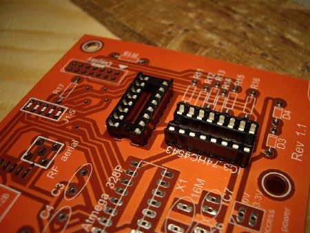
NB. When the pin-saving hardware is in use, no wire links should be fitted at the J1-J5 connector.
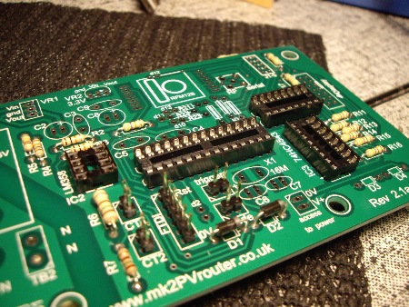
NB. The two ICs which comprise the pin-saving hardware were both initially specified from the 74HC series. Unfortunately, the 74HC4543 for IC3 is no longer available in DIL form. When operated at 3.3V, the replacement CMOS part is not able to provide the necessary drive capability. So whenever the pin-saving hardware is to be used, the processor must be operated at 5V.
The remaining components can be assembled in any convenient order. In all cases, I would recommend only attaching one lead for each component initially; the alignment can then be checked and adjusted as necessary before the rest of them are soldered into place.
In the next photo, I am about to fit the 16 MHz crystal. This component is indicated on the silk-screen layer as X1.
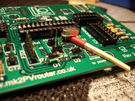
A matchstick can be put to good effect for this purpose. Here, some heat-shrink sleeving has been used to increase the matchstick's thickness.
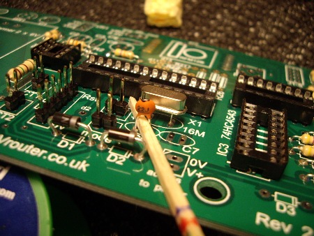
Here, a thinned matchstick is being used to hold one of them away from the board prior to soldering.
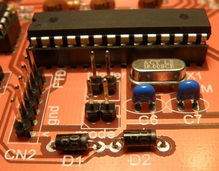
Thanks to Bill Thomson in Oklahoma for his photo of this board.
By bending their legs tightly, these diodes have been fitted close to the board.
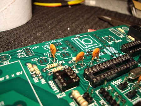
It provides some protection for the delicate radial components when the PCB is inverted.
This component needs to go the correct way around, as indicated on the silk-screen layer.
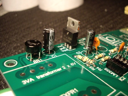
The DC power supply has four components, all of which need to be fitted in the correct orientation:
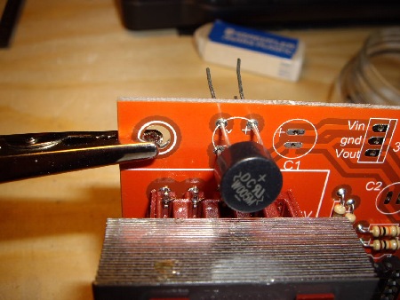
The longest leg is marked '+' on the can and also on the silk-screen image.
Trimming the legs to different lengths makes this component much easier to fit.
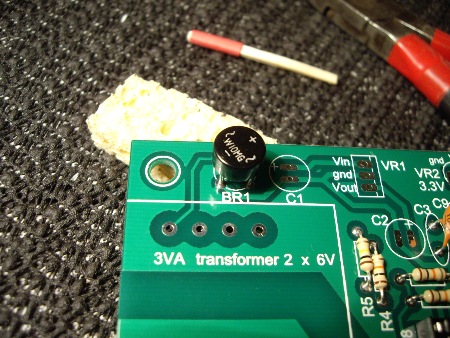
I now prefer to leave the transformer until the end of the assembly sequence.
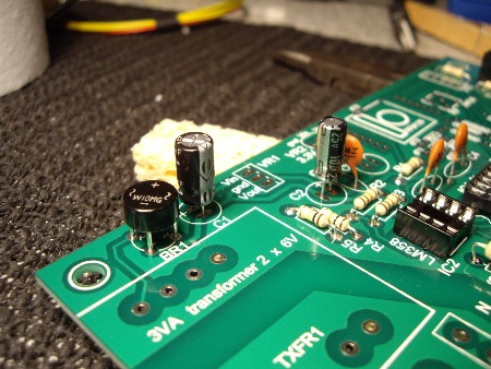
The -ve pin is indicated by a prominent stripe running the length of the component.
The other pin is the +ve one, which must go into the hole marked '+' on the silk-screen image.
NB. Although they look fairly similar, it is important that these two capacitors are fitted in the correct locations. The larger capacitor (C1 = 100 μF) is closest to the bridge rectifier. The smaller one (C2 = 10 μF) is nearest to IC2. If these two components are swapped over, the resulting symptoms can be difficult to diagnose.
The voltage regulator (VR1) must be fitted with its metal fin away from the transformer as shown on the silk-screen layer . Depending on the application, VR1 will either be a 3.3V or a 5V device. 5V is needed whenever the pin-saving hardware is in use.
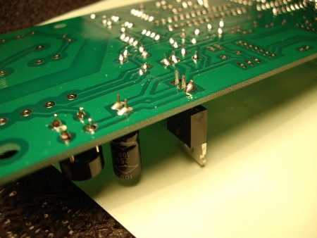
To reduce the amount of metal to be heated, I pre-cut these leads to the required length.
Leaded solder, which melts at a lower temperature, may be helpful for these connections.
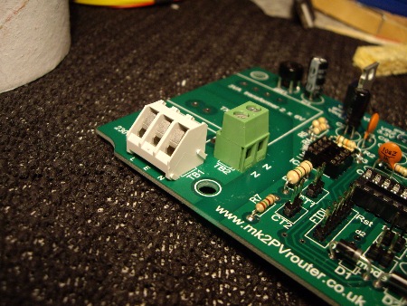
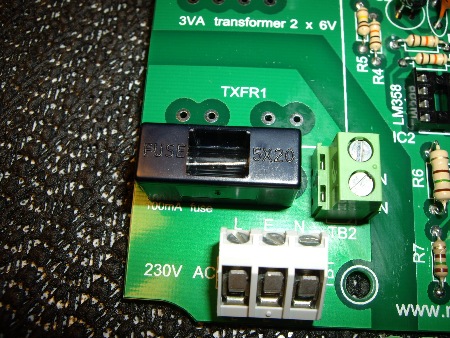
These terminal blocks must be oriented correctly to allow easy access to the wiring. It's all too easy to get them the wrong way around!
If this happens, the plastic can be carefully trimmed away with a knife, and each pin extracted separately.
I have plenty of spare connectors …
The final component to be fitted is the transformer. This is generally a dual 6V device as shown on the silk-screen layer. A 6V transformer can support either a 3.3V or a 5V voltage regulator. Two different types of transformer have been used for this project. The Blore Bowron type, usually labelled "JPR Electronics 835-401", was used on all boards up to Rev 2.1a. The Myrra equivalent was introduced at Rev 4.1.
WARNING! - The transformer is a fragile component which needs to be treated with care.
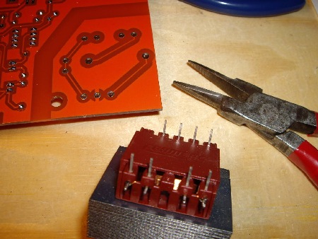
Take care not to damage the fine wire which is attached to most of these pins.
The primary winding - which runs between the two outer pins on this side of the transformer - is particularly fragile.
The resistances of the three windings on the dual 6V Blore Bowron transformer are:
primary coil ~1300 ohms; secondary coils ~4 ohms.
The next three images relate to the Blore Bowron transformer which has proved to be particularly fragile.
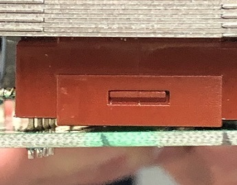
I learned this lesson the hard way ...
The board shown here was fine during my tests but then failed after being shipped to a customer. During transit, the poorly retained transformer was able to move on its pins and the fine wire of the primary coil became severed.
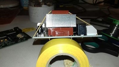
Here, I have used an elastic band but insulating tape could be equally effective.
Note the absence of any gap this time.
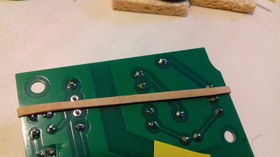
The final two pins could then be soldered without any danger of the transformer moving.
With the transformer in place, the board is now ready for electrical testing. This is a good time to check that all the soldered joints look OK and that any solder splashes have been removed.
Before fitting any of the ICs, the operation of the power supply needs to be checked.
Safety Warning:
To continue with this build sequence, access to 230V mains voltage is required. Please do not proceed to this next stage unless you are competent to do so.
In the photo below, I have connected a temporary 230 V AC supply via a 3-Amp fuse. Although not required by this PCB, the Earth core provides a degree of safety in the event of the operator accidentally coming into contact with the 230 V AC line.
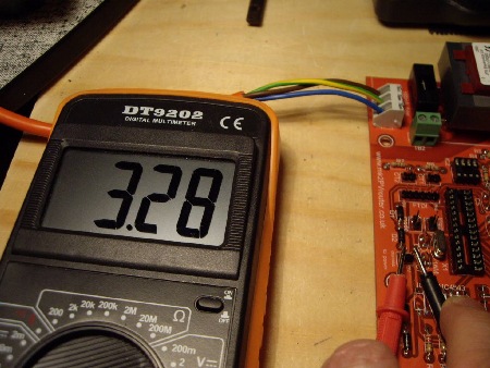
… or 5V if a 5V voltage regulator has been fitted.
This voltage can be conveniently checked at the "access to power" connector, as shown here.
Other than the transformer, which may feel slightly warm after several minutes, none of the components on the board should show any noticeable increase in temperature.
With the correct voltage in place, the ICs can now be fitted. The first of these is IC2. This is an op amp which provides a mid-rail reference voltage for the voltage and current sensors.
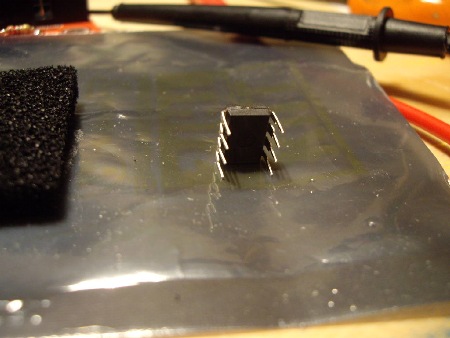
This can be done by gently 'rolling' the chip on each side in turn.
To minimise the risk of electrical damage, this operation should be done on a protective surface such as an anti-static bag.
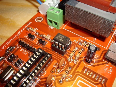
ICs need to be fitted the correct way around. The dot on the chip must align with the notch in the silk-screen image.
When everything has been carefully checked, the chip can be pressed firmly home.
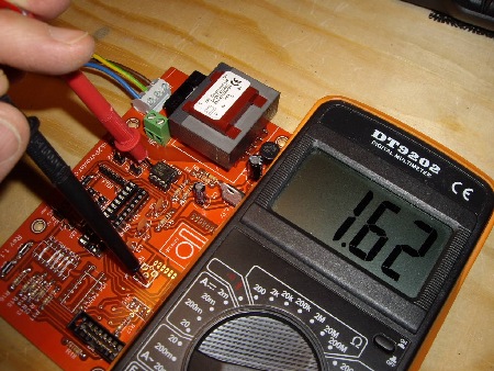
Vref should be approximately half of the supply voltage. Here I am testing a 3.3 V board.
A convenient place to access Vref is at the upper end of R6. The SMA jack-socket is a convenient earth.
Vref can also be accessed at various other places, as shown on the circuit diagram for this board.
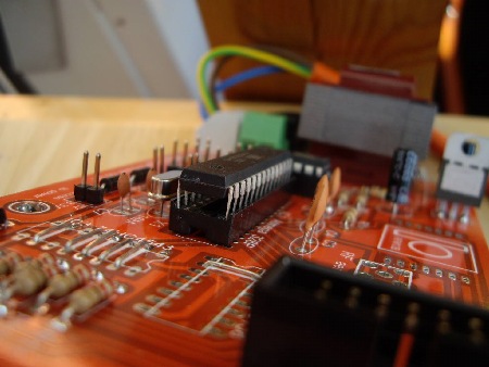
With so many pins, it's all to easy for one of them to get bent underneath.
Warning: if this IC is the wrong way around when power is applied, it will most likely never work again!
With the processor in place, it may be a good idea to check that the power supply is still OK. Assuming that is it, let's run a sketch (program) to establish whether the processor is working.
For this next stage, a suitable programming facility will need to be in place. Details about how to set up the Arduino Integrated Development Environment (IDE) can be found at the top of this page.
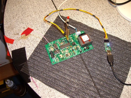
A USB-to-USART programmer will need to be plugged onto the FTDI connector on the PCB as shown below. The other end of the programmer needs to be connected via a suitable USB lead to the programming facility (PC or equivalent).
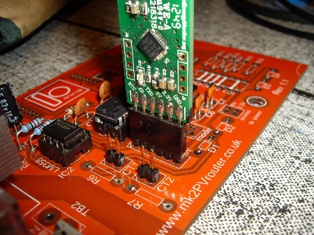
This is an old version of the Open Energy Monitor (OEM) programmer.
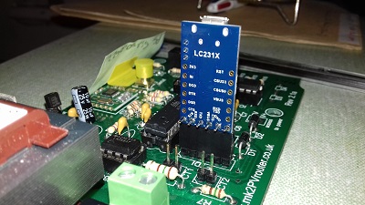
The "Gnd" pin must always be closest to the edge of the board
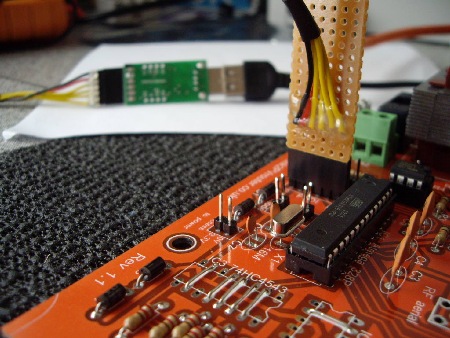
Only four of the lines are actually used (Tx & Rx data, ground, and reset). Neither of the power lines are used by this board.
The black wire is for the GND (or OV) connection.
The transformer has two outputs: one is for the DC supply, the other is for the AC voltage sensor which should already be working. This can be verified by running a programme (sketch) which displays the analogue measurements that are being taken by the Atmel processor (IC1).
The software sketch, which is also on the Downloads page, is: RawSamplesTool_2chan.ino
[NB. When a file is downloaded from this website, it is automatically "opened" within a suitable editor or browser. To use a software sketch, the entire content of the displayed file should be copied and saved as a local file using the name that appears here. Because it has the suffix ".ino", that file will then be recognised as an Arduino source file by the Arduino IDE].
Having uploaded this sketch to the processor via the Arduino IDE, the Serial Window (magnifying glass icon) needs to be opened within a few seconds, otherwise the action will be missed. After completing each run, the sketch can be re-started from the keyboard by entering the character 'g', followed by [CR].
The RawSamplesTool_2chan sketch displays the AC voltage and current samples for one or more complete mains cycles. If a sizeable current is being measured as well as the voltage, the displayed results will look more interesting.
Here is some output that I captured when measuring the current drawn by a 3 kW load with my CT plugged into CT2. When the CT was moved over to the CT1 port, the resulting output looked almost identical but with the '1' and '2' characters swapped over.
If no signals are available at the CT1 and CT2 ports, the waveforms for those channels will both be straight lines. Only the voltage signal will display a sinusiodal appearance. To check the operation of the CT1 and CT2 ports while the PCB is being tested on the bench, some suitable wiring will be needed.
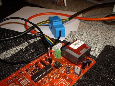
The external CT normally plugs into a 3.5mm jack-socket in the wall of the enclosure. The signal gets to the PCB connector via an adapter with green & yellow wire as shown in this image from the System Assembly page.
To check the operation of individual IO ports such as the "mode" port (D3) or the "trigger" port (D4), a simple sketch such as "blink.ino" can be used. This can be found in the Examples section of the Arduino IDE (File → Examples → Basics).
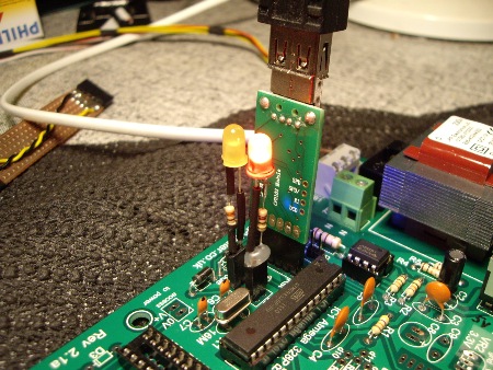
Each one is just an LED with a series resistor.
A simple sketch to exercise D4 is on my Downloads page as "blink_dig4.ino".
Formal testing of the 4-digit display is described in the Assembly & Testing page. When checking a completed PCB in isolation, I have a functional but blemished display assembly which can be used for this purpose as shown below.
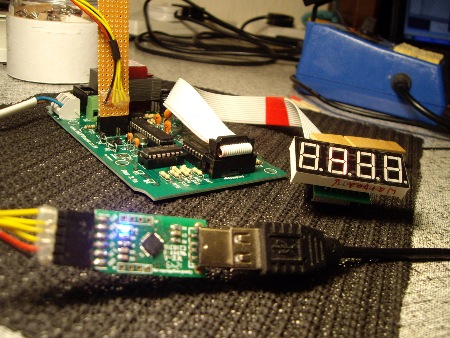
Although not evident in this photo, the display was cycling through its test sequence at the time.
It therefore needs to operate at 5V so R4 is 180R and R11-R18 are 470R.
When you've reached this stage, Congratulations - you now have a working main board.
∗ ∗ ∗
If the RF facility is required, an RFM12B module will need to be fitted to the board. This device requires a power supply of 3.3V which may or may not already be available on the PCB.
If the processor is running at 3.3 Volts (i.e. VR1 = 3.3V), a simple wire link between the 'Vin' and 'Vout' pins at VR2 will extend this voltage to the RF module. Additional links at R24 - R26 are needed to connect three of the digital control lines. With these four links in place, the board is ready for the RFM12B device to be fitted.
Testing was achieved by connecting a linking cable to an adjacent PCB on which the power supply was present.
The on-board PSU can supply power to a second PCB if necessary.
If, however, the main processor is running at 5 Volts, a step-down stage will be required for the RF module. This involves the fitting of nine extra components as shown below.
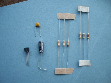
VR2: 3.3V, TO-92
C8: 10 μF
C9: 0.01 μF (1E4 pF)
R21-R23: 10 K
R24 - R6: 4K7
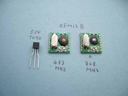
The 433 MHz variant of the RFM12B has an extra capacitor. The absence of this capacitor on the 868 MHz variant is indicated in this photo.
My supplier uses gold & silver paint to identify these two different variants after testing.
These extra components for the RF stage (other than the RFM12B module itself) are fitted in a straightforward manner.
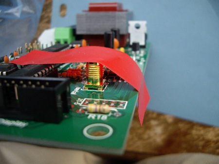
Be wary of overheating this component lest the internal insulation could be damaged.
With everything else in place, the final component to be fitted is the RFM12B module.
Warning about the risk of Electro-Static Damage (ESD)
The RFM12B module is a static-sensitive component which could be easily damaged if handled incorrectly. The modules that I supply have been tested and sealed into individual anti-static pouches. Please ensure that suitable precautions are taken when fitting this component, particularly if working in hot dry conditions.
While the RF module is held in the correct place by any convenient means, e.g. a sliver of doubled-sided tape, each wire is connected as shown in the following sequence. The next two photos were taken using a prototype board, but the method of mounting the RF chip has not changed since then.
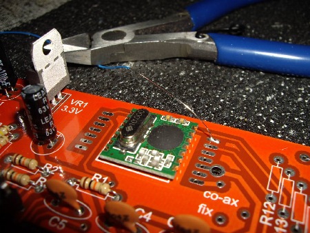
This needs to be retained by some temporary means while being soldered into place from above …
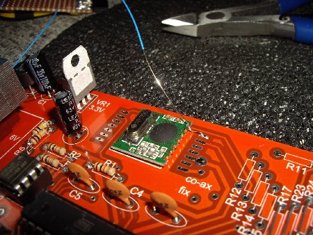
Wires are only needed for 8 of the possible 14 locations as shown in the photo below.
Finally, any excess wire is trimmed away from both above and below the board.
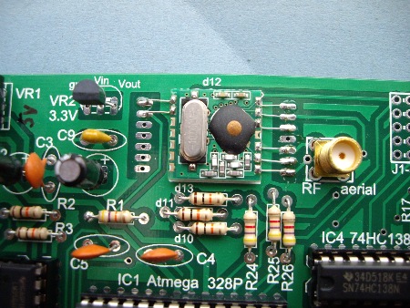
To avoid any possible confusion, it's a good idea to write the frequency of the module onto the PCB. There are some photos here that should help to identify the different modules and frequencies.
(I have yet to do that for this board)
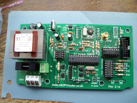
This board will operate at 5V, hence the extra 3.3V power supply stage and the presence of R21 - R26.
If it were a 3.3V board, four wire links would be needed: one at VR2, and three at R24-R26.
Of the eight wires that are connected to the RFM12 module, five are for digital IO ports D2 and D10 - D13 which are then dedicated for this purpose. The remaining three wires are for the power rails and the aerial.
A quarter-wave aerial for 433 MHz is 165 mm; for 868 MHz it is 82 mm.
(Aerial details here)
Parts list for the 1-phase PCB:
| Identity on PCB | component description | # used | notes |
|---|---|---|---|
| (none) | 1-phase PCB, Rev 4.1 | 1 | |
| 2VA txfr | transformer 2 x 6V | 1 | Myrra 44163 |
| (none) | fuse (100mA), slow blow | 1 | 20 x 5 mm |
| 100mA fuse | fuseholder | 1 | |
| TB1 | terminal block, 3-way, angled | 1 | |
| TB2 | terminal block, 2-way, straight | 1 | |
| BR1, BR2 | bridge rectifier | 1 | |
| VR1 | 3.3V or 5V voltage regulator | 1 | TO-220 |
| X1 | crystal, 16 MHz | 1 | |
| C6, C7 | capacitor, 22 pF ceramic | 2 | |
| C3-C5 | capacitor, 100 nF ceramic | 3 | |
| C2 | capacitor, 10 uF electrolytic | 1 | |
| C1 | capacitor, 100 uF electrolytic | 1 | or 220uF for 5V use |
| Atmega 328P | processor, Atmega 328P | 1 | |
| IC1 | DIL socket, 28-pin | 1 | for IC1 |
| LM358 | op amp, LM358 | 1 | |
| IC2 | DIL socket, 8-pin | 1 | for IC2 |
| D1-D6 | diode, 1N4007 | 6 | |
| R1 | 0.25 Watt resistor, 47K | 1 | |
| R2, R3 | 0.25 Watt resistor, 10K | 1 | |
| R4 | 0.25 Watt resistor, 100R | 1 | or 220R for 5V use |
| R5 | 0.5 Watt resistor, 1K0 | 1 | |
| R6 | 0.5 Watt resistor, 120R | 1 | or a different burden resistor value |
| R7 | 0.25 Watt resistor, 120R | 1 | or a different burden resistor value |
| R8 | 0.25 Watt resistor, 1K0 | 1 | protection against over-current |
| R11-R18 | 0.25 Watt resistor, 220R | 8 | or 470R for 5V use |
| various | SIL pin strip (0.1", 18-way) | 1 (typ) | for FTDI, CTs, IO ports, LEDs |
| various | SIL socket, 2-way | 4 (typ) | for CTs and IO port connections |
| Display | boxed header, 14-way | 1 | |
| RF components: | |||
| RFM12B | RFM12B or RFM69CW | 1 | 433 or 868 MHz |
| RF aerial | SMA receptacle | 1 | |
| pin-saving hardware: | |||
| IC2 | DIL socket, 14-pin | 2 | for IC3 & IC4 |
| CD4543 | 7-segment decoder | 1 | IC3 |
| 74HC138 | 3->8 Decoder | 1 | IC4 |
| for a dual supply board: | |||
| VR2 | 3.3V regulator, small (TO-92) | 1 | |
| C8 | capacitor, 10 uF electrolytic | 1 | |
| C9 | capacitor, 100nF ceramic | 1 | |
| R21-R23 | 0.25 Watt resistor, 10K | 3 | |
| R24-R26 | 0.25 Watt resistor, 4K7 | 3 |
